Coherent X-ray Scattering Masks

Note: This page has migrated to new file space on the SSRL server. If you find a broken link you can browse the updated:

 sample folder directory.


Metal Deposition Details


Gold Selective Etching


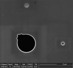
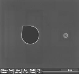
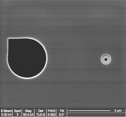
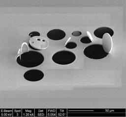
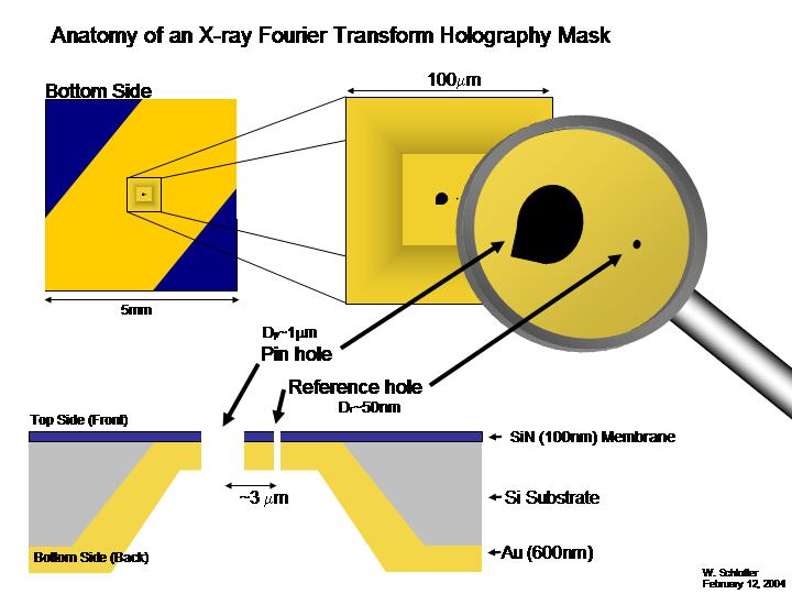
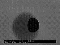
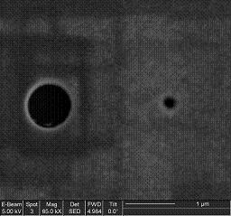
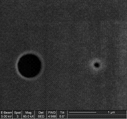
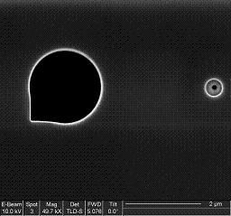
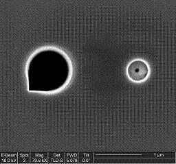
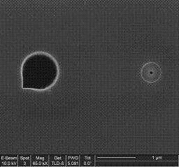
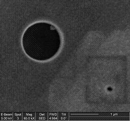
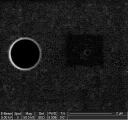
Illustratio ns that explain terms used in the following pages


C1 (used for practice milling)


C2 (never milled)


C3 BESSY


C4 (never milled)


C5 (never milled)


C6


C7 (never milled)


C8 (never milled)


C9  BESSY


C10 (Dose array)


C11 (never milled)


C12 (never milled)


C13  (Dose array)


C14  (Selective etch rate test) 


C15  (Integrated magnetic multilayer) BESSY (sent FedEx Feb. 7)


C16 (Integrated magnetic multilayer) BESSY (sent FedEx Feb. 7)


C17  BESSY (delivered by Jan)


C18    BESSY  (delivered by Jan)


C19   BESSY (sent FedEx Feb. 7)


C20


C21 (Integrated magnetic multilayer) BESSY (sent FedEx Feb. 7)


C22 (USED FOR DOSE ARRAY) (Integrated magnetic multilayer)


C23 (Integrated multilayer) (similar to C21) BESSY (sent FedEx Feb. 7)


C24< /a> (Similar to C18, but better)  BESSY (sent FedEx Feb. 7)


C25  (Integrated multilayer)


C26  (Two reference holes)


C27


C28


C29


C30  Coherence hole d=20 microns  (Sent to BESSY August 2004)


C31 Coherence hole d=10 microns (Sent to BESSY August 2004)


C32  Coherence hole d=50 microns


C33 Coherence hole d=100 microns

< /p>


C34 Coherence hole d=10 microns


C35 Coherence hole d=20 microns


C36    ; Dose array


C37   Dose array


C38  Selective etch test


C39  Nitride under sample hole, reference hole penetrates Au and Nitride  (sent to Jülich Oct. 10, 2004)

Sample hole diameter 2000nm


C40  Both holes penetrates Au and Nitride  (sent to Jülich Oct. 10, 2004)

Sample hole diameter 2000nm


C41 Both holes penetrates Au and Nitride  (sent to Jülich Oct. 10, 2004)

Sample hole diameter 2000nm


C42 Both holes penetrates Au and Nitride  (sent to Jülich Oct. 10, 2004)

Sample hole diameter 5000nm


C43 Both holes penetrates Au and Nitride  (sent to Jülich Oct. 10, 2004)

Sample hole diameter 5000nm


C44 Selective etch


C45 Etch test


C46 e4633 Dose Array


C47 e4633a Dose Array


C48 e4633b Dose Array


C49 Reference hole penetrates Au/SiN/multi layer(e4633)   (sent to BESSY Oct. 24, 2004)


C50 Reference hole penetrates Au/SiN/multilayer(e4633a)   (sent to BESSY Oct. 24, 2004)

The original reference hole didn't penetrate so the redrill is on the right


C51 Reference hole penetrates Au/SiN/multilayer(e4633b)   (sent to BESSY Oct. 24, 2004)


C52  Double pinhole for coherence measurement (sent to BESSY Oct. 24, 2004)

No multilayer


C53


C54  Selective etch test for new Gold Target used in Metallica #5   v5p69-91


C55   Selective etch test for new Gold Target used in Metallica #5  (Shattered Chip) v5p73-78


C56     Metallica #6 test and Rectangular aperture test for URA  v5 p92


C57     Metallica #6 test for chips sent to Konstanz v5p96-100


C58 &n bsp;   Metallica #7 Dose testing, cross sections and focus tests v6 p 4-6, 11-16


C59     Integrated  Multilayer (e4 645)  Only one reference hole penetrated  v6 p19-21


C60     Gold Coated Dust     (e4656d)


C61   &n bsp; Integrated  Multilayer (e4556d)  Excellent reference holes.  v6 p21-22


C62    Integrated  Multilayer (e4541)  Excellent round reference holes.  v6 p21-22


C63  Integrated  Multilayer (e4556s)  v6 p32


C64  Integrated Multilayer sample e4641, but the gold didn't mill well see vol. 6 p33


C65  Integrated Multilayer sample e4556s, but the gold didn't mill well see vol. 6 p33


C66  Dose Array for Nanoparticles


C67  Sample with 110nm nanospheres see vol 6 p 57


C68 Sample with 110nm nanospheres see vol 6 p 59


C69 


C70  Dose Array for 2 micron gold for double pinholes and small squares   see WFS v7p6-12  


C71  Double Pinhole with 3 microns center to center    see WFS v7 p13/15, RRv1p6 


C72   Double Pinhole with 5 microns center to center    see  WFS v7 p16, RRv1p7 


C73  Double Pinhole with 7 microns center to center  WFS v7 p17, RRv1p8 


C74  Double Pinhole with 1 microns center to center


C75 Double Pinhole with 1 microns center to center


C76 Double Pinhole with 9.8  microns center to center


C77 Double Pinhole with 19.8  microns center to center


C78 URA sample   WFS V7 p27


C79 No sample


C80 Dose array Metallica#9  and e4973 WFS V7 p47 p55(small holes)


C81 Metallica#9 test sample  WFS V7 p58-59


C82 M9 e4974 see doc in folder   WFS V7 p??


C83 Bio particle injection, see doc in folder   WFS V7 p?


C84 Bio particle injection, see doc in folder   WFS V7 p?


C85 Bio particle injection, see doc in folder   WFS V7 p6?


C86 Bio particle injection, see doc in folder   WFS V7 p?


C87  Broken window


C88 Five Reference, F object, M9,M10,M11  WFS V7 p72,83


C89 Extended Field of View F TH M9,M10,M11    WFS V7 p74 with map on p92


C90 Dose array M9 and M11   WFS V7 p89


C91 Large Crisp Reference sample,    WFS V7 p83 map on V8 p11


C92 Astigmatic Reference sample,   WFS V7 p99 map on V8 p8


C93 Dose array with only M11   WFS V7 p99


C94 Double Object Extended Field of View   WFS V8p7 map V8 p8


C95 No sample


C96  Dose array for M12 and e5092    WFS V8 p38


C97  M12 and e5092    WFS V8 p53


C98  M12 and e5092    still on wafer


C99  


C100  M12 and e5091    WFS V8 p50


C101  M12 and e5091    still on wafer


C102  M12 and e5091 &nb sp;  still on wafer


C103 58nm Nanospheres WFS V8 p40


C104 58nm Nanosphere Dosearray


C105 58nm Nanosphere 3 Object Hole


C107 58nm Nanosphere Object Hole missed


C108 M12 with 320nm spheres WFS V8 p66


C109 M13 patterned media  WFS V8 p59


C110 M13 patterned media


C111 Patterned Media


C112 M13 patterned media

< hr>

C113 M13 patterned media


C114 M13 patterned media


C115 No SC e5071 M13 WFS V8 p66


C116  SC, e5071, M13 WFS V8 p63 with map


C117  SC, 2ndMag Layer, e5071, M13 WFS V8 p63 with map


C118 No SC, e5066 ,M13 WFS V8 p65


C119 SC, e5066 ,M13 WFS V8 p62 with map


C120 SC, 2ndMag Layer, e5099, M13 WFS V8 p61 with map


C121 e5066 ,M13 WFS V8 p65


C121a 70um Pinhole (originally thought to be NRA2)


C122  WFS V6 p1


C123 NRA II   WFS V8 p67,76-78


C124


C125 Thin Domainwalls - Pentagon Dosearrays


C126 Thin Domainwalls - 1 Objecthole, 4 of Ref Hole Pentagon penetrated, added 2nd object hole 1.5um 2 Ref holes penetrated


C127 Thin Domainwalls - 1 Objecthole, 0 of Ref Hole Pentagon penetrated originally, now 5 ref holes penetrated - added 2nd refhole 1.5um, 2 ref holes penetrated


C128 Small Pinhole 400nm Diameter on frontside


C129 (wants to be) Small Pinhole 120nm Diameter on frontside
Stripe comes from intermediate UHR SEM Picture.
UHR's effect on ibeam decays wit h ~5s time constant.


C130 M9 (Tohru Sample A)  WFS V8 p90,94 (membrane broke in ultrasonic bath)


C131 M9 (Tohru Sample B)  WFS V8 p91 wit h map, p92,p93 


C132 Thick Co mask SC-002 - Dosearrays

Thickness estimate FIB-SEM: maybe 395 or 353, i.e. 370+-40nm


C133 Thick Co mask on front, SC -002 - unused.


C134 Thick Co mask on front, SC-002 - unused.


C135 Thick Co mask on front, SC-002, Thin Co Mask on back SC-003. - unused.


C136 Thick Co mask on front, SC-002, Thin Co Mask on back SC-003. - unused.


C 137 Thin Co mask on front, SC-003

Objecthole punched through, 5 Ref holes, 3 penetrated smallest 30x30nm


C138 Thin Co mask on front, SC-003 - unused.


C139 Thin Co mask on front, SC-003 - unused.


C140 Thin Co mask on front, SC-003 - unused.


C141 Thin Co mask on front, SC-003 - unused.


C142 Fe mask on front, SC-004

Crosssection and cracked films

Thickness FIB-SEM: 265+-40nm


C143 Fe mask on front, SC-004 - unused - Membrane deformed & broken.


C144 Fe mask on front, SC-004 - unused - Membrane deformed & broken


C145 Aperture D=47um M4+M5+M7 (3.7um of Au)   WFS V9 p15


C146 Aperture D=5.3um M4   WFS V9 p14


C14 7  M11  


C148 100nm SiN mebrane to practice beamstop deposition and frame cut  WFS V9 p16,18,19


C149 500um x 300um membrane 150nm SiN broke after a few take one ion images WFS V9 p23


C150 2.5mm x 5mm membrane 50nm SiN broke on first take one ion images WFS V9 p22


C151 Patterned Beamstop, M2 (2-3nm of Cr and Au) 500um x 300um membrane 150nm SiN, ~1um particle on surface WFS V9 p26


C152  Aperture D=1um M4+M5+M7 (3.7um of Au)   WFS V9 p27 with map on p28


C153 M9, e4976 angled reference holes  


C154 AFM with CNT on omniprobe (not a real chip)    WFS V9 p24


RR V2 p9&10


C155 Met14 - SiN Terassing Test (Metallica) rr V1 p61,79ff


C157  polymer nanospheres wfs v9 p44


C158 Met14 - Goal> 200n m Obj hole, Refholesrr V1 p61, 83


C159  Aperture D=10um M4+M18 (~5um of Au)   RR V1 p84-87


C159_bill  patterned beamstop disk  wfs v9 p47


C160  Aperture D=45um M4+M18 (~5um of Au)   RR V1 p84-87


C161>  Aperture D=1um M4+M5+M7 (~5um of Au)   RR V1 p84-87


C161_bill  patterned AFM tip for reflection experiments wfs v9 p62


C162>  Metallica 17, FePt Nanoparticles 1mg/ml   RR V1 p95-96

2 Object Holes with pentagon refhoses. (old p1,p2) Not a single ref hole made it through.

P2: 20deg Terassed Objecthole 0.3-0.9um + 15 References a 15-50nm at 4.5um, ~half of ref holes made it though

P2

P2

P2


C163>  Metallica 17, FePt Nanoparticles 0.1mg/ml   RR V1 p95 M17 DOSEARRAY !!!!!!!!!!!!!


C164>  Metallica 17, FePt Nanoparticles 1mg/ml   RR V1 p95 V2

P1: Non Terrassed Object hole 170nm + 5(3) References a 18nm at 1um

P2: Non Terrassed Object hole 170nm + 3 References a 18nm, One 20, one 30 at 1um

P3: 30deg Terrassed Object hole 0.46-1.8um + 3 References a 40nm at 2.25um

P4: 20deg Terrassed Object hole 0.3-0.9um + 15 References a 50-30nm at 4.5um

P5: 20deg Terrassed Obj ect hole 0.3-0.9um + 7 References a 40nm at 3um

P1

P2

P3

P4

P5


C165>  Metallica 17, FePt Nanoparticles 5ul of 1mg/ml - Microflanch (9 Ref holes from Nitride Side after terassing. off center object hole    RR V1 p95 V2 p5-6


C166 >  Metallica 17,   RR V1 p95

P1: Object hole .17um no references

P2: Object hole .9-1um punched through no references

P3: 20deg terrassed Object hole 0.3-0.9um, 2-4 Monolayer NP Patch, + 7 References a 40nm at 3um

P3


C167>  Metallica 17, FePt Nanoparticles 1mg/ml   RR V1 p95


C168>  Metallica 17, FePt Nanoparticles 5ul of 1mg/ml   RR V1 p95, V2 p17-19

P1: 30deg Terassed Objecthole 0.46-1.8um + 9 References a 45-60nm (oval) at 3um (Overlap in Autocorrelation)

P2: 30deg Terassed Objecthole 0.46-1.8um + 9 References a 45-60nm (oval) a t 3um (Overlap in Autocorrelation)

P3: 30deg Terassed Objecthole 0.46-1.8um + 15 References a 45-60nm (oval) at 3um (Overlap in Autocorrelation)


C169>  Metallica 17, FePt Nanoparticles 5ul of 1mg/ml   RR V1 p95


C170>  5nm Cr 10nm Au, FePt Nanoparticles 40ul of 1mg/ml on .3x.5mm Membrane -> 1 to 4 FePt Monolayers    RR V2 p11


C171>  e5342, Metallica 19, Dosearray    < /font>RR V2 p28


C172>  e5352, Metallica 19, made sample A4, A6, A8, Object Holes On Target    RR V2 p28ff


C173>  e5356, Metallica 19, has 50um long crack at side of membrane plus 40um Diameter Hole in membrane all of this is about 180 to 200um away from the patterns (usable in principle) -> nothing done so far    RR V2 p28ff


C174>  e5356, Metallica 19, made sample A4, A6, A8, Objectholes off Target    RR V2 p28ff


C175>  e5356, Metallica 19, Patterns blocked by dust particle    RR V2 p28ff


C176>  e5352, Metallica 19, Crack in SiN - not on Membrane tho ugh - still usable    A6 Objecthole 40nm Islands, Object Diameter 352-1035nm, 3 Reference Holes 27x26, 26x22, 30x30 RR V2 p28ff, RR V2 p84f


C177>  e5348, Metallica 20, Dosearray   ;  RR V2 p42ff


C178>  e5384, Metallica 20, Several Objectholes, some broken through others misplaced.    RR V2 p42ff


C179>  e5381, Metallica 20, made sample A4, A6, A8 Oval Ref holes ~40x80nm    RR V2 p42ff


C180>  e5384, Metallica 20, made sample A4, A6, A8 Ref holes ~40nm - BESSY Sample CoPt+Fe   

RR V2 p42ff


C181>  e5382, Metallica 20, made sample A4, A6, A8 Ref holes ~40nm - BESSY Sample CoPt   

RR V2 p42ff


A51>  Metallica 19, Magnetic triangle, Object hole at one corner /   KC


C188 extended field of view sample with corners  (M19?)  Just  800nm of Au


C194>  SC032&Metallica?, 10nmAu, 50nmCo, 30nmCr, 100nmSiN, 800nmAu Resonant Phasing Sample RR V2 p80ff


C200>  25um Guardhole, 4um Gold, Metallica 25 RR V2 p88


C201>  10.5um Guardhole, 4um Gold, filled w/ Si Paste in the meantime RR V2 p90


C202>  Big Si Chunk w/ 4 broken Membranes to test fixing with Silver Paint or White out. Si Paint works if used in small amount. White out was definitely much too. RR V2 p94f


C203>  M26, Olav Samples 44,44A RR V2 p95


C204>  M26, Olav Samples 44,44B RR V2 p95


C205>  M26, Olav Samples 43,43A RR V2 p95


C206>  M26, Olav Samples 43,43B RR V2 p95


C207  M27, Olav Samples 44,44c Broken membrane


C208>  M27, Olav Samples 44,44d Broken membrane


C209>  M27, Olav Samples 77,77a oval reference holes


C210>  M27, Olav Samples 77,77b dose array


C211>  M27, Olav Samples 77,77c


C212>  also R001


C213>  also R002


C214>  also R003


C215>  also R4, Double Pinhole Array, RR V3 p2


C216>  also R5, Double Pinhole Array, RR V3 p2


C217>  also R6, 5um guard hole in 4um Au


C218>  also R7, Double Pinhole Array, RR V3 p3


C219>  also R8, Double Pinhole Array, RR V3 p3


C220>  also R9, "inverted sample", Fire, Dirty chip


C221>  also R10, Dosearray


C222>  also R11, "inverted sample", Pi


C223>  also R12, "inverted sample", Tree


C224>  also R13, "inverted sample", Fire


C225>  also R14 unused


C226>  Olav samples / Hitachi, O454_1


C227>  Olav samples / Hitachi, O454_2


C228>  Olav samples / Hitachi, O455_1


C229>  Olav samples / Hitachi, O455_2


C230>  Olav samples / Hitachi, O455_3


C231>  Olav samples / Hitachi, O594_1


C232>  Olav samples / Hitachi, O594_2


C233>  Olav samples / Hitachi, O594_3


C234>  Olav samples / Hitachi, O594_4


C236>  M27, Nanocubes 30nm<\p>


C237>  M27, Nanocubes 30nm<\p>


C238>  M27, Nanocubes 30nm<\p>


C239>  M27, Nanocubes 30nm<\p>


C240>  M27, Nanocubes 30nm<\p>


C241>  M27, Nanocubes 30nm<\p>


C242>  M27, Nanocubes 30nm<\p>


C243>  M27, Nanocubes 30nm<\p>


C244>  M27, Nanocubes 30nm<\p>


C245>  M27, Nanocubes 30nm<\p>


Upload details:

Path   $WEB:[ROOT.STOHRGROUP.FIB]

Use reflection x FTP client with windows