Organic semiconductor materials have some intriguing advantages compared to their inorganic counterparts: low-cost and versatile manufacturing (e.g. roll-to-roll printing), material abundance and new form factors (e.g. flexible, transparent and stretchable). However, solution-processed organic devices are usually made and optimized with poorly scalable fabrication using lab-based techniques such as spin coating or dip coating. A better route for organic-electronics fabrication is printing, which can potentially realize large-area, high-throughput, low-cost fabrication on an industrial scale.

Single-crystalline thin films are the ideal form of organic semiconductors for achieving high-performance electronics owing to the high degree of coherent transport in these structurally nearly perfect materials. With single-crystalline films the orientation of the film relative to the electrical contacts becomes important because charge transport is highly dependent on the crystal orientation, i.e. along certain directions electrons and holes move with great ease whereas along other directions transport may be slow due to a lower electronic coupling between the molecules in that direction. The ultimate goal of forming aligned single crystals directly through solution printing and coating has so far not been achieved.
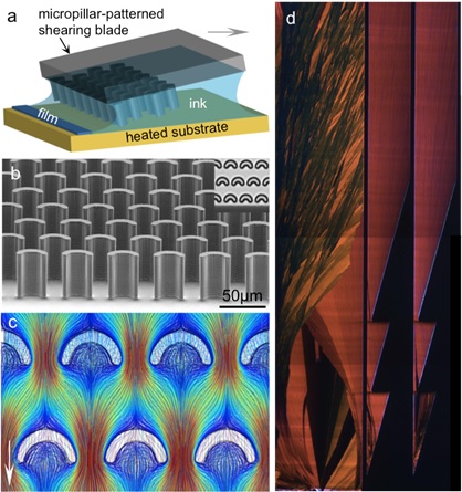
In this study, supported by the Department of Energy and the Laboratory Directed Research and Development Program, scientists from Stanford University, Nanjing University (China) and SSRL report a new method, called FLUENCE (fluid enhanced crystal engineering), for fabricating aligned single crystals. The method is generally applicable to large-scale coating and printing processes. The essence of FLUENCE is the control of fluid flow during crystal formation. Structural imperfection is commonplace during rapid solution printing. FLUENCE tackles this problem from two angles. First, FLUENCE introduces dense arrays of micro-structures on the printing blade (Figure 1a) to facilitate the formation of ink films with uniform concentration during the printing process. This is critically important since without these structures, the limited mass transport within the ink leads to very inhomogeneous, typically dendritic growth of the crystallites. Second, FLUENCE tunes the curvature of the ink–substrate interface to quench the stochastic nucleation of the crystal grains. This part of the method is inspired by the effect that nucleation preferentially happens in places where the ink meniscus is highly curved – an explanation which not too long ago also explained the well-known “coffee ring effect” [1,2]. The combination of these two approaches in the FLUENCE method leads to large-area, highly-aligned single-crystalline thin films with an unprecedented degree of structural perfection.
The degree of alignment in the FLUENCE-printed single-crystalline films and their structural perfection were analyzed in-depth using SSRL Beam Lines 11-3, 7-2, 1-5 and 2-1. Using X-ray scattering profiles and line width analysis, the research team found a massively reduced spread in crystallite orientation (from around 60 degrees in films printed without FLUENCE to 2 degrees in FLUENCE-printed films), and very high degree of structural perfection in the films (800 nm coherence length) that rivals values published for slowly and vapor-grown large crystals of these materials.
This work is the first demonstration of simultaneous control of crystal alignment, molecular packing structure and deposition of single crystals over a large area. This level of control is unprecedented for solution coating. The electrical performance of FLUENCE-printed films of the commercially available organic semiconductor TIPS-pentacene is raised from the typical value reported for solution-deposited films of this material (1-2 cm2/Vs) to a record value of 11 cm2/Vs (hole mobility). This result serves as an example for the potentially huge performance benefit for organic devices that comes from a material delivery that is directly engineered to address the existing issues in solution-formed films. The engineering solutions developed in this work were derived though a critical analysis of the physics (microfluidics, thermodynamics and kinetics) that govern the film formation from ink in the printing process.
The concepts demonstrated in FLUENCE can be easily scaled and transferred to commercial printing methods. The significant improvement in the structural quality and electrical performance of the films printed with the FLUENCE method could enable the production of small, inexpensive organic circuitry with lower power consumption and higher performance.
1. R. D. Deegan, O. Bakajin, T. F. Dupont, G. Huber, S. R. Nagel, T. A. Witten, "Capillary Flow as the Cause of Ring Stains from Dried Liquid Drops", Nature 389, 827 (1997).
Y. Diao, B. C.-K. Tee, G. Giri, J. Xu, D. H. Kim, H. A. Becerril, R. M. Stoltenberg, T. H. Lee, G. Xue, S. C. B. Mannsfeld, Z. Bao, “Solution Coating of Large-area Organic Semiconductor Thin Films with Aligned Single-crystalline Domains”, Nat. Mater. 12, 665 (2013), DOI: 10.1038/nmat3650.

