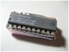
The need for reliable and secure technological devices requires integrated circuits (ICs) that maintain integrity of the original design1. In order to keep costs low, ICs are often manufactured overseas2. Chip modifications, also called “Hardware Trojans” can be inserted in various phases of production, testing, and distribution, and be triggered later by pre-programmed timed or physical events, which can cause failure or compromise at key times during operation3. This can affect applications in fields as diverse as defense, aeronautic industry, consumer medical and financial records, and transportation security, for example. The authentication of IC chips to scan for Trojans can be complex because the type of modification can vary significantly, and is usually unknown in advance. Hence a thorough yet non destructive method for ensuring circuit integrity is required.
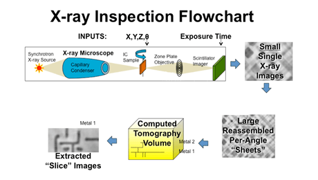
Using the transmission x-ray microscope on Beam Line 6-2 at the Stanford Synchrotron Radiation Lightsource, based on an Xradia lab model4, researchers from the University of Southern California Information Sciences Institute and Xradia Inc. have developed nanoscale computerized tomography (CT) methods to obtain nondestructive high resolution (30 nm) 3D images of integrated circuits that could be used to scan for defects and modifications. Because the ICs are very large compared with the microscope field of view (30 microns), complex methods for imaging of the circuits and reconstruction of the 3D data were developed (Figure 1).

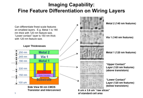
Because a 2D transmission image will reveal all absorbing objects penetrated by the x-ray path, tomography is necessary to combine views from different angles and reveal the different layers in the IC chip. A quick and robust method is required for scanning of chips, because of the large amounts of images required to cover a full chip area. Image registration algorithms are used to align multiple raster-scanned images at each angle, and then to align the tomographic data set with multiple angles. After image acquisition and reconstruction to form a 3D volume, individual layers of the chip could be distinguished with a 3D visualization program. Slice imaging detail, which could be viewed and inspected for changes from the original design, is shown below in Figure 2 and in the movie. The synchrotron x-ray energy can also be tuned to image above and below the x-ray absorption edge of specific metals within the chips to view gate and active areas, and back end wiring interconnect layers.

In summary, the use of x-ray nanotomography for imaging of electronic circuits, on a scale of high automation and accuracy, could enable high-throughput screening of IC chips used in critical applications in which failure could compromise critical capabilities or information. Imaging results from this project have been published in the Proceedings of the 36th GOMACTech Conference.
Virtual Delaying of Integrated Circuit in 90nm Technology Using X-ray Computed Tomography from SSRL on Vimeo.
Acknowledgments
This work was sponsored by the Defense Advanced Research Projects Agency Microsystems Technology Office (MTO) Program “Enhancing trust with X-ray Phase-Optimized Scanning Equipment (EXPOSE), ARPA Order No. X040/07, Program Code: 7720 Issued by DARPA/CMO under Contract No. HR0011-07-C-0102. “The views and conclusions contained in this document are those of the authors and should not be interpreted as representing the official policies, either expressly or implied, of the Defense Advanced Research Projects Agency or the U.S. Government.” Special thanks also to the support of Stanford / SSRL including Piero Pianetta, Joy Andrews Hayter, and Sean Brennan, who spent many hours assisting with our experimental setup.
1. Pope, S., Trusted Integrated Circuit Strategy. IEEE Transactions on Components and Packaging Technologies 31 (1), 230-234 (2008).
2. Defense Science Board Task Force on High-Performance Microchip Supply, Report (2005). Office of the Undersecretary of Defense, Washington DC.
3. Karri, R., Rajendran, J., Rosenfeld, K. and Tehranipoor, M. ,Trustworthy Hardware: Identifying and Classifying Hardware Trojans. IEEE Computer MagazineOctober 39-46 (2010).
4. Tkachuk A., Feser M., Cui H., Duewer F., Chang H., Yun W., High-Resolution X-ray Tomography Using Laboratory Sources, in Developments in X-ray Tomography V, ed. Ulrich Bonse, Proc. of SPIE 6318, 63181D (2006).
M. Bajura, G. Boverman, J. Tan, G. Wagenbreth, C. M. Rogers, M. Feser, J. Rudati, A. Tkachuk, S. Aylward, P. Reynolds “Imaging Integrated Circuits with X-ray Microscopy” Proceedings of the 36th GOMACTech Conference, March 2011, Orlando, FL.

