Conjugated polymers are being developed as the active semiconductor in devices such as light-emitting diodes, photovoltaic cells, and thin-film transistors (TFTs) for large-area and low-cost electronics. Vacuum deposited amorphous silicon is currently used in the TFTs that drive the active matrix liquid crystal displays (AM-LCDs) on laptops, computer monitors and televisions. TFTs are also used in disposable electronics such as radiofrequency identification chips. Solution processible conjugated polymers, such as the polythiophenes, can be deposited by low cost methods like inkjet and screen printing. The charge carrier mobility (0.1 cm2/Vs) of the standard polythiophene, poly(3-hexylthiophene) (P3HT), is just below that of amorphous silicon (0.6 cm2/Vs). To open up more applications and to better compete with amorphous silicon, the mobility of polymer semiconductors needs to be improved. The key to improving the mobility is to develop an understanding of the relationship between polymer morphology and charge transport.

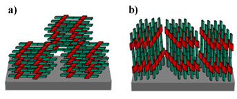
Previously, Sirringhaus et al. have used grazing incidence x-ray scattering (GIXS) (Nature 401, 685 (1999)) to show a correlation between the orientation of P3HT crystals and the charge carrier mobility. Films with crystals primarily oriented with their side chains normal to the substrate and the chain backbone and the π-faces in the plane of the substrate (edge-on) had higher mobility than those oriented with their π-faces normal to the substrate and the side chains and chain backbone in the plane of the substrate (plane-on) as shown in figure 1. Since the π-faces and the chain backbone are the only directions that transport charge (the side chains are insulators), the edge-on orientation was said to provide two-dimensional charge transport. Using beamlines 7-2 and 2-1 to study the polymer morphology with GIXS and specular diffraction rocking curves, a team of researchers from SSRL and Stanford have shown that the increase in charge transport associated with the transition from edge-on to plane-on orientation is largely due to changing the nature of the grain boundaries. Crystals with a plane-on orientation have grain boundaries terminated with insulating alkyl chains on two sides, effectively blocking charge transfer to neighboring crystals.
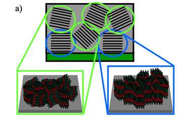
Rocking curves showed the unexpected presence of highly oriented grains in the polymer films (figure 2). These grains were oriented within 0.03 degrees of the substrate normal (resolution of the instrument). Conventional understanding for the semicrystalline films would have expected orientation distributions of 5-20 degrees. The highly oriented crystals were shown to have nucleated from the dielectric substrate, the critical interface where all the current in a TFT travels. The concentration of these highly oriented crystals was directly correlated to the charge carrier mobility of P3HT films by varying the surface modification of the substrate with self-assembled monolayers. Making the silicon oxide surface hydrophobic by treating it with octadecyltrichlorosilane gave the best results. The strength of the surface effect on the charge carrier mobility was dependent on the molecular weight (MW) of the P3HT. Low MW P3HT exhibited the strongest correlation with surface treatment (1000x) while high MW P3HT showed very little dependence on the surface treatment. These results provide a better understanding of the polymer morphology that lead to high mobility films.

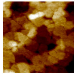
This same team of researchers in collaboration with scientists from Merck Chemical and the Palo Alto Research Corporation (PARC) have revealed a new polymer, poly(2,5-bis(3-alkylthiophen-2-yl)thieno[3,2-b]thiophenes)) (PBTTT), with the highest reported charge carrier mobility (0.7 cm2/Vs) to date, making it competitive with amorphous silicon. Measurements at SSRL and Stanford showed the polymer to have the highest crystallinity ever observed for a semiconducting polymer. The edge-on orientation of the polymer crystals was enhanced by annealing the films in the liquid crystalline regime. Atomic force microscope images (figure 3) of these films showed crystal domain sizes on the order of 200 nm, almost an order of magnitude larger than any previously observed in semiconducting polymers. The specular diffraction intensity was also over an order of magnitude higher than the best P3HT films. These results showed that the films consisted entirely of the highly oriented crystals first observed in P3HT. The researchers have shown the polymer to have a similar morphology to what is seen in small molecules despite having polymer chains 40 times longer.
"Highly Oriented Crystals at the Buried Interface in Polythiophene Thin Film Transistors", R.J. Kline, M.D. McGehee, M.F. Toney, Nature Materials 5, 222-228 (2006).
"Liquid crystalline semiconducting polymers with high charge carrier mobility", I. McCulloch, M. Heeney, C. Bailey, K. Genevicius, I. MacDonald, M. Shkunov, D. Sparrowe, S. Tierney, R. Wagner, W. Zhang, M.L. Chabinyc, R.J. Kline, M.D. McGehee, M.F. Toney, Nature Materials 5, 328-333 (2006).

