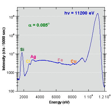
 Increasing the speed and complexity of semiconductor integrated circuits requires advanced processes that put extreme constraints on the level of metal contamination allowed on the surfaces of silicon wafers. Such contamination degrades for example the performance of the ultra thin SiO2 gate dielectrics (< 4nm) that form the heart of the individual transistors. Ultimately, reliability and yield are reduced to levels that must be improved before new processes can be put into production. Much of this metal contamination occurs during the wet chemical etching and rinsing steps required for the manufacture of integrated circuits and industry is actively developing new processes that have already brought the metal contamination to levels beyond the detection capabilities of conventional analytical techniques. The measurement of these extremely low contamination levels has required the use of synchrotron radiation total reflection x-ray fluorescence (SR-TXRF), and sensitivities about 50 times better than those of conventional laboratory instruments have been achieved at BL6-2 of SSRL. Figure 1 shows a typical TXRF spectrum of a "clean" silicon wafer. The spectrum has been measured for 5000 s with an x-ray incidence angle of 0.085° for high surface sensitivity, which is well below the critical angle for total external reflection. The most intense feature dominating the background in the high energy region of the spectrum is the elastic and inelastic scattering of the incident SR. In the low-energy part of the spectrum, the Si Kα fluorescence signature from the substrate is clearly visible. The overall shape of the fluorescence spectrum below 7 keV is characteristic of Bremsstrahlung emission creating background in the low energy part of the spectrum.

This results from the interaction of the primary incident photons with the silicon substrate itself. At 6-9 keV, the spectrum shows the signature of process-related contamination from Cu and Fe. On the basis of a calibration standard, the Cu concentration is 2.6x10⁸ atoms/cm2 and the Fe concentration 6.4x10⁸ atoms/cm2. This can be translated into a minimum detection limit for transition metals of 8x10⁷ atoms/cm2 for a standard 1000 s counting time, which corresponds to a detection limit of 1 fg distributed over an area of 14 mm2 on the wafer surface [1,2]. Even for the best commercially available conventional TXRF instrument based on a rotating anode, this Cu concentration is well below its minimum detection limit and, as a result, the wafer would appear as completely clean.
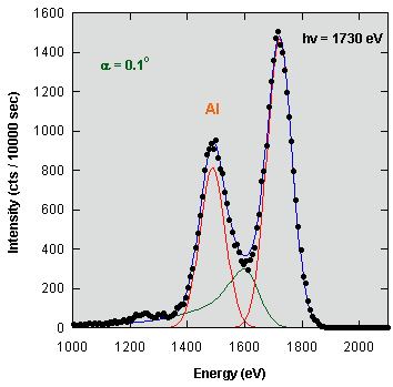
Apart from the detection of transition metals, SR-TXRF can also be extended to detecting elements with Z < 14, of particular importance is Al. This is not only challenging because of the smaller fluorescence yield as compared to transition metals, but especially because of the much stronger Si substrate fluorescence signal, which cannot be attenuated by a cut-off filter and therefore easily dominates the spectrum and saturates the semiconductor detector. Only exploiting the tunability of SR and choosing an excitation energy below the Si K absorption threshold can overcome these limitations. However, as shown in Figure 2, a substantial increase in background due to inelastic x-ray Raman scattering is observed. This background limits the minimum detection limit for Al, which has been derived for a bending magnet beam line to be 7.6x10⁹ atoms/cm2 for a standard 1000 s counting time [3].
Furthermore, the chemical state of device impurities can be investigated at trace levels by combining TXRF with x-ray absorption near edge spectroscopy (XANES) to monitor fluorescence yield as a function of excitation energy. Especially in case of semiconductor surfaces, the effect of an impurity strongly depends on its oxidation state and it is demonstrated that this technique will eventually contribute to the development of more efficient wafer cleaning processes.

This research was carried out at the Stanford Synchrotron Radiation Laboratory, a national user facility operated by Stanford University on behalf of the U.S. Department of Energy, Office of Basic Energy Sciences.
- K. Baur, S. Brennan, P. Pianetta, R. Opila, Anal. Chem. 74, 609-616 (2002).
- P. Pianetta, K. Baur, A. Singh, S. Brennan, J. Kerner, D. Werho, J. Wang, Thin Solid Films 373, 222-226 (2000).
- K. Baur, J. Kerner, S. Brennan, A. Singh, P. Pianetta, J. Appl. Phys. 88, 4642-4647 (2000).

