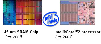
Scaling of conventional silicon based metal-oxide-semiconductor (MOS) transistors requires thinner and thinner SiO2 films. However, the increase of leakage current through thinner SiO2 films puts a fundamental limit on the existing MOS technology. High dielectric constant (high-k) materials are natural substitutes for SiO2 as insulators because they can maintain sufficient thickness to achieve desired capacitance. In fact, hafnium based high-k dielectric materials are already used by Intel in the fabrication of the current generation of 45 nm SRAM chips and processors (Figure 1).
The increasing need for higher speed and lower power consumptions has pushed Si-based transistors to their performance limit. III-V compound semiconductors, due to their high carrier mobility, are very promising in replacing Si as substrates of semiconductor chips. Various combinations of high-k dielectric films on III-V substrates are being actively evaluated. However, sufficient valence and conduction band discontinuities between the high-k insulator and the semiconductor substrate are necessary to act as barriers for both electron and hole injection. Therefore, before a particular high-k insulator is selected for semiconductor chip it is very important to know the band offsets between it and the semiconductor substrate.

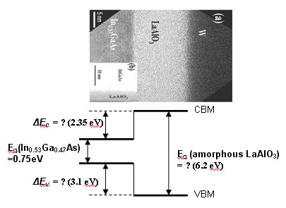
In this work, high-k dielectric LaAlO3 films on In0.53Ga0.47As substrates were grown at Intel and studied at Stanford Synchrotron Radiation Lab (SSRL). As shown in figure 2, only the band gap of the In0.53Ga0.47As substrate is already known. To find out how the bands are aligned, we needed to establish the valence band offset DEv and the band gap of the amorphous LaAlO3 film, both of which were measured by photoelectron spectroscopy at beam line 8-1 and beam line 10-1 of SSRL.
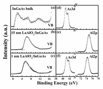
Valence band offset can be obtained by comparing the valence band maximum (VBM) of LaAlO3 and In0.53Ga0.47As, as shown in figure 3. However, because LaAlO3 is an insulator, positive charge will be built up on the surface when photoelectrons are emitted. This positive charge will cause the whole spectrum to shift. To correct this shift, a sample with thin (1 nm) LaAlO3 film is prepared because we can collect both As 3d and Al 2p core levels from this sample. These two core levels are used as references to align with the As 3d of the clean
In0.53Ga0.47As sample and the Al 2p of the sample with thick (15 nm) LaAlO3 film, respectively. After the spectra are properly aligned and the spectral shift caused by surface charging is corrected, the valence band offset is determined as 3.1 eV.

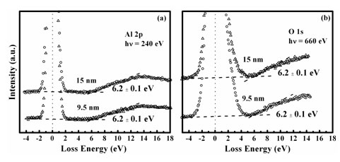
The band gap of LaAlO3 is traditionally determined by optical measurement. However, the band gap of LaAlO3 film is generally different from that of bulk LaAlO3. In addition, it is found that band gaps of high-k dielectric films are also significantly affected by film growth conditions. Therefore, we can not rely on previously published LaAlO3 band gap data. In this work, we use the energy loss features of Al 2p and O 1s core levels to measure the band gap, as shown in figure 4. This energy loss feature creates a slope on the higher binding energy side of the background. The energy difference between the onset of the slope and the core level peak position is the band gap. Here, the band gap of the LaAlO3 film is measured as 6.2 eV. Consequently, the conduction band offset is calculated to be 2.35 eV. These measured and calculated numbers are shown in parenthesis in figure 2.
The band offset measurements, in theory, can also be done using conventional UPS and XPS instead of synchrotron sources. In reality, several problems with conventional sources make it very difficult. For example, UPS can measure the valence band, but lack of core level information makes it impossible to align the spectra in order to correct the charging effect. For the band gap measurement, the energy loss feature is very weak, and therefore, for a reliable quantification it is necessary to have a very flat background and narrow core level peak. In a conventional XPS system the photon energy is not tunable and the spectral resolution is poorer, making it virtually impossible to identify the onset of the slope caused by the energy loss feature. Therefore, because of the high collimation and very high-resolution, coupled with continuous tenability of the photon energy, XPS systems operating at synchrotron sources are ideally suited to study the band offsets between thin films and substrates.

Band gap and band offset measurements are not only very important for addressing the viability of newer generation of semiconductor chip technology, but they are also of vital importance in the study of materials used in solar energy technologies, which are actively investigated in SSRL as well. The techniques highlighted here pave the way for investigations of many technologically important electronic devices.
N. Goel, W. Tsai, C.M. Garner, Y. Sun, P. Pianetta, M. Warusawithana, D.G. Schlom, H. Wen, C. Gaspe, J.C. Keay, et. al. (2007) Band offsets between amorphous LaAlO3 and In0.53Ga0.47As. Applied Physics Letters, 91, no.11, p.113515

