
Understanding Charge Transport in Plastic Electronics
Recent advances in materials research are setting the stage for macroelectronics to have a disruptive effect on everyday technology. While microelectronics focuses of the miniaturization of electronic devices (think of the shrinking iPod), macroelectronics is the replication and integration of microelectronic devices onto large areas such as display backplanes (big screen TVs and electronic billboards), large-area photovoltaics (flexible solar cells) and radio frequency ID tags. One class of materials that has demonstrated great promise as the semiconducting layer in these macroelectronics devices is polymer semiconductors, which allow for potentially inexpensive manufacturing from solutions.
Often, thin films of these polymer semiconductors are semicrystalline, consisting of small regions or grains where the molecules are ordered; these grains are separated by grain boundary regions where molecules are amorphous or disordered. It is believed that charges can easily traverse the crystalline grains, but are hindered by the disrupted structure at the grain boundaries. By understanding exactly how the grain boundaries slow charge transport, the polymer film microstructure can be engineered for improved performance.
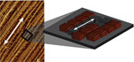
Researchers at Stanford University, including graduate student Leslie Jimison and Prof. Alberto Salleo, collaborated with SSRL staff scientist Mike Toney to perform x-ray diffraction experiments at SSRL Beam Lines 11-3 and 7-2. The researchers investigated the properties of unique, aligned thin films of semicrystalline poly(3-hexylthiophene) (P3HT). Diffraction data gave insight into film microstructure, including orientation of chains within grains and possible grain boundary structure. In one direction of the anisotropic film, there is the potential for polymer chains in adjacent crystallites to cross the grain boundaries, which may make these grain boundaries less detrimental to transport. Electrical measurements of thin film transistors confirmed that charge transport is indeed more efficient in directions where this is more likely to occur.
Results in this work help strengthen the understanding of the relationship between polymer film microstructure and semiconductor performance by giving insight into how crystalline orientation, which defines grain boundary structure, can be optimized for efficient charge transport in electronic devices. This work was published in the April 27 issue of the journal Advanced Materials.
To learn more about this research see the full Scientific Highlight
"Orientation of Regioregular Poly(3-hexylthiophene) by Directional
Solidification: A Simple Method to Reveal the Semicrystalline Structure of a
Conjugated Polymer" M. Brinkmann, J. Wittmann. Adv. Mater. 18, 860 (2006).
"Transport in polycrystalline polymer thin-film transistors" R. Street, J.
Northrup, A. Salleo. Phys. Rev. B. 71, 13 (2005).
