
Semicrystalline polymers, such as polythiophenes, hold much promise as active
layers in printable electronic devices such as photovoltaic cells, sensors, and
thin film transistors. As organic semiconductors approach commercialization,
there is a need to better understand the relationship between charge transport
and microstructure, in particular, to identify the inherent bottlenecks to
charge transport. In semicrystalline and polycrystalline materials, charge
transport is most likely dominated by grain-boundary effects, although the
exact mechanism is not well understood. Unfortunately, grain boundaries in
semicrystalline thin films are difficult to characterize: the grains are too
small to allow for measurements across individual grain boundaries (as is often
done for polycrystalline films of small molecules) and bulk measurements are
complicated by the unknown orientation of polymer chains within the grain. To
better understand the effect of chain orientation on grain boundaries, we use
anisotropic thin films of poly(3-hexylthiophene) (P3HT) - one of the most
well-studied polymeric semiconductors, as a tool to study charge transport.
We characterized the film microstructure and made thin film transistors with
the anisotropic film as the active layer. This allowed us to quantitatively
extract the effect of different grain boundary structures on charge transport
and showed for certain low-angle grain boundaries, charge transport is due to
bridging polymer molecules. Our study shows that optimization of the
microstructure in semicrystalline electronic devices should include efforts to
control grain boundary structure and orientation.
From our diffraction experiments, we were able to develop a model of the film
microstructure, shown in Figure 1, right. By collecting diffraction data from
only the crystalline regions, we have obtained indirect information about the
structure at the grain boundaries. It has been previously suggested that in
polymeric semiconductor films, grain boundaries separating two grains with a
small orientation mismatch, known as "low-angle" grain boundaries, can contain
bridging polymer chains that create favorable paths for intergrain charge
transport. Our films are comprised entirely of low-angle boundaries, but due to
the orientation of the polymer axis, boundaries along the fibers, or "in-line"
boundaries, are more likely to have bridging polymer chains than boundaries
between fibers. To test the effect of these boundaries on charge transport, we
made thin film transistors (TFTs) using the anisotropic film in two different
orientations, one with fibers parallel to the channel length along which the
current flows (parallel devices) and the other with fibers perpendicular to the
channel length (perpendicular devices.) The mobility values for the two types
of devices revealed a significant mobility anisotropy: parallel devices had
mobilities approximately 20 times higher than perpendicular devices (Figure 3).
In fine-grained materials such as the directionally crystallized films of P3HT,
the effective device mobility is dominated by the mobility in the grain
boundaries. Thus, the mobility anisotropy in the semicrystalline films studied
here is attributed to different microstructure at the grain boundaries.
Transport across grain boundaries along the fiber, with the potential for
bridging polymer chains, is easier than transport across the fibers.
Additionally, similar activation energies, extracted from temperature dependent
mobility measurements (Figure 3, inset), indicate that despite mobility
anisotropy, charge transport in the two types of devices is governed by the
same transport bottleneck. We believe that due to film imperfections, grain
boundaries between fibers play a role in both types of devices, serving as the
rate limiting step.
In summary, we have created anisotropic films of P3HT via directional
crystallization and used them as a tool to study the effect of grain boundary
structure on charge transport. Film microstructure was largely characterized
using X-ray diffraction at SSRL, and charge transport was investigated by
making thin film transistors with the anisotropic films as the active layer.
This work helps to solidify the hypothesis that in low-angle grain boundaries,
transport is easier only in the direction parallel to the polymer backbone, due
to bridging polymer molecules. Optimization of the microstructure in electronic
devices should therefore not focus solely on the elimination of grain
boundaries, but also include efforts to control grain boundary placement and
relative grain orientation.
"Charge Transport Anisotropy Due to Grain Boundaries in Directionally
Crystallized Thin Films of Regio-Regular Poly(3-hexylthiophene)", L.H. Jimison,
M.F. Toney, I. McCulloch, M. Heeney, A. Salleo. Adv. Mater. 21,
1568-1572 (2009).
Primary Citations
"Orientation of Regioregular Poly(3-hexylthiophene) by Directional
Solidification: A Simple Method to Reveal the Semicrystalline Structure of a
Conjugated Polymer" M. Brinkmann, J. Wittmann. Adv. Mater.
18, 860 (2006).
"Transport in polycrystalline polymer thin-film transistors" R. Street, J.
Northrup, A. Salleo. Phys. Rev. B. 71, 13 (2005).
Anisotropic thin films of P3HT are fabricated by a directional crystallization
technique adapted from Brinkmann and Wittmann (see reference for fabrication
details). The behavior of the films under polarized light suggests widespread
alignment of the polymer chains, with the chain axes parallel to the fiber
axis. Atomic Force microscopy reveals areas of continuous, aligned films, and
suggests the presence of grains along the fibers (Figure 1, left). X-ray
diffraction experiments at SSRL Beam Lines 11-3 and 7-2 were used to
characterize the semicrystalline microstructure of the anisotropic films more
directly. Two-dimensional grazing incidence X-ray scattering (2D GIXS) survey
patterns (Figure 2a) reveal the unique texture of these P3HT films. Typical
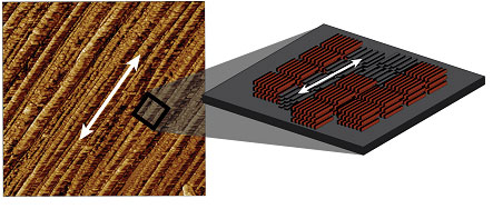
Figure 1:
Phase mode AFM image of directionally crystallized P3HT, revealing the unique
grain structure. The white arrow indicates the direction of the fiber axis and
polymer chain axis. The scan is 4 by 4 mm. (Left) The cartoon shows a possible
orientation of crystallites within the directionally crystallized film, as
derived from XRD. Red crystallites are "edge-on" with their pi-pi stacking
repeat in the plane of the substrate. Grey crystallites are termed "face-on,"
with their pi-pi stacking repeat out of the plane of the substrate. In this
cartoon of the grains, the longest axis is long the polymer chain backbone
(001), the next longest along the alkyl-stacking direction (100) and the
shortest along the pi-pi stacking direction (010), see Figure 2b for reference.
(Right)
spin-cast thin films of P3HT are highly textured out of plane, with the
alkyl-stacking repeat direction lying out of the plane of the substrate and the
resulting (h00) peaks appearing along the qz axis. In the
directionally crystallized films, the peak corresponding to the pi-pi stacking
appears out-of-plane, along with weaker (h00) peaks (see Figure 2b for
reference). The presence of both of these Bragg peaks along the
qz axis
indicates that there is a distribution of crystallites present in our films,
"face-on" and "edge-on," as shown in the right hand side of Figure 1.
High-resolution GIXS experiments were performed at two different substrate
orientations, probing repeat distances both along the fibers and across the
fibers. The difference in these diffraction patterns confirms significant
in-plane crystalline anisotropy. The Bragg peaks that are present in the GIXS
patterns also confirm the orientation of the chain axis along the fiber axis,
and two different crystallite orientations, as suggested above.
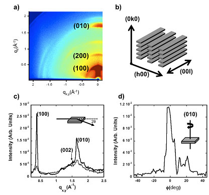
Figure 2:
a) Grazing Incidence X-Ray Diffraction (GIXD) survey pattern of directionally
crystallized P3HT, revealing the unique thin film texture. b) A representative
crystallite of P3HT, for reference. c) High resolution grazing incidence X-ray
diffraction, taken in two different sample orientations (phi). The thick black
line corresponds to a scattering vector oriented across the fibers. The thin
black line corresponds to a scattering vector oriented along the fibers. d) A
phi scan of the (010) peak, quantifying in-plane film anisotropy.
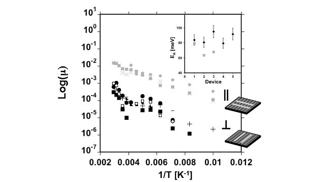
Figure 3:
Temperature dependent mobilities for perpendicular (black) and parallel (grey)
devices. The different symbols correspond to different devices. Inset:
Activation energies extracted from the temperature dependent mobilities. Error
bars for the parallel devices are smaller than the symbols.
Further Reading
SSRL is supported by the Department of Energy, Office of Basic Energy Sciences. The SSRL Structural Molecular Biology Program is supported by the Department of Energy, Office of Biological and Environmental Research, and by the National Institutes of Health, National Center for Research Resources, Biomedical Technology Program, and the National Institute of General Medical Sciences.