
Nanoporous or mesoporous inorganic materials with homogeneous pore sizes have
found broad applications in separations, as supports for size selective
catalysis, and as low dielectric materials. For all of these applications, it
is the pore space that is important, and so the inorganic framework is
 |
generally formed from a simple material like silica or another oxide. In an
effort to extend the range of potential applications for this class of porous
materials, research at the University of California, Los Angeles (UCLA) have
recent shown that solution phase templating routes can be used to form ordered
nanoporous versions of classic semiconductors such as germanium.
Surfactant templating is a method that has been successfully employed to
produce nanoporous inorganic structures from a wide range of oxide-based
material. Co-assembly of inorganic precursors with amphiphilic organic
molecules is followed first by inorganic condensation to produce a rigid
amorphous framework and then by template removal to produce a mesoporous solid.
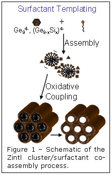
In a new advance to this field, researchers at UCLA have shown that it is
possible to use surfactant-driven self-organization of soluble Zintl clusters
to produce periodic, nanoporous versions of classic semiconductors such as
amorphous Ge or Ge/Si alloys. They specifically employed derivatives of the
anionic Ge94- cluster, which was co-assembled with
cationic surfactants to produce an ordered nanostructured composite. Oxidation
of the reduced Zintl clusters to neutral germanium cross-linked the germanium
framework and released the cationic surfactant, resulting in a periodic porous
semiconductor with a pore diameter of ~3 nm and surface areas as high as 500
m2/g. The inorganic/surfactant co-assembly process is shown
schematically in figure 1.
 |
To understand the mechanism of self-assembly and to characterize their
materials, UCLA researchers used a combination of many experiments, including
transmission electron micro-scopy (TEM), X-ray diffraction, X-ray photoelectron
spectroscopy (XPS), and gas porosimetry. An example of TEM images of some of
the materials are shown in figure 2. One other particularly useful
characterization tool was germanium extended X-ray absorption fine structure
(EXAFS). EXAFS experiments were carried out at beam lines 4-1 and 6-2 at SSRL.
The experiments allowed the UCLA researchers to understand the local structure
in their composite materials before and after oxidation and to confirm that the
final porous materials contained tetrahedrally bonded germanium, just like bulk
amorphous germanium.
While most of the work to date has focused on developing the fundamental
self-organization required to produce these materials, a broad range of new
applications are potentially enabled by these materials. They both absorb and
emit light at near infra-red wavelengths. Moreover, the band gap can be tuned
both by tuning the thickness of the germanium walls (an effect known as quantum
confinement) and by changing the composition of the framework. For example, by
analogy with bulk group IV semiconductors, if the Zintl clusters made from a
mixture of silicon and germanium are used, the resulting porous material has a
significantly blue shifted band gap. The materials also appear to conduct
electricity almost as well as bulk amorphous germanium, despite their
nanoporous architecture. UCLA researchers are currently exploring a variety of
applications for these materials, including nanoscale solar cells and
adsorption based chemical sensors. Because the semiconductor surface is
exposed and accessible in these materials, they have the potential to interact
with a variety of species in ways that could eventually lead to a range of
novel nanostructured devices.
Primary Citation
"Hexagonal Nanoporous Germanium through Surfactant-Driven Self-Assembly of
Zintl Clusters" D. Sun, A.E. Riley, A.J. Cadby, E.K. Richman, S.D. Korlann, and
S.H. Tolbert, Nature, 441, 1126-1130, (2006).
|
