Porous nanoscale materials often have useful properties because of their
proportionally large surface areas. Now, UCLA scientists have devised a way to
make porous germanium, a semiconductor used in fiber optics and electrical
components. This discovery means that nanoporous materials could soon be used
to develop new kinds of solar cells or highly sensitive electronic sensors.
Until now chemists have had difficulty forming germanium that contains
regularly spaced, nanoscale holes. Previous nanoporous materials were made from
oxides, which are ideal for use as catalysts but have only a narrow range of
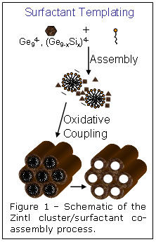
usefulness in electronics. Using a technique called "surfactant templating,"
UCLA chemist Sarah Tolbert and colleagues combined a soap-like molecule, or
"surfactant" with a special preparation of germanium molecules. Under the right
conditions these two components mix and arrange themselves into a honeycomb
lattice. The new compound is chemically treated to remove the surfactant,
leaving a skeleton of germanium with very thin walls.
Porous germanium prepared in this way has an enormous surface area - 500 square
meters per gram. That makes it ideal for use in highly sensitive sensors and
detectors, in which tiny traces of a material must adhere to a surface to be
detected.
Tolbert and her team used several approaches, one of which being extended x-ray
absorption fine structure (EXAFS) techniques at SSRL's Beam Lines 4-1 and 6-2,
to characterize these new nanoscale structures.
To learn more about this research see the full scientific highlight at:
http://www-ssrl.slac.stanford.edu/
research/highlights_archive/Ge.html
"Hexagonal Nanoporous Germanium through Surfactant-Driven Self-Assembly of
Zintl Clusters" D. Sun, A.E. Riley, A.J. Cadby, E.K. Richman, S.D. Korlann, and
S.H. Tolbert, Nature, 441, 1126-1130, (2006).