Figure 1. PbTiO3 nanostructures onto
(100) SrTiO3 substrates. Topography
image obtained by Scanning Force Microscopy (SFM), showing nanosized and
uniform PbTiO3 particles with a short range one dimensional
periodicity detected by the Fast Fourier Transform of the topography image.
In the literature two methods for fabrication of ferroelectric nanostructures
have been reported; top-down, i.e., lithography-based patterning and a
bottom-up approach based on self-assembly. The first approach provides good
spatial resolution and positioning precision, but at present is very expensive.
A further limitation of this approach is that fabricated structures cannot be
easily made much smaller than ~100 nm laterally. Bottom-up methods are low-cost
and allow a relatively easy fabrication of structures with sizes below 100 nm,
but the issues of organization and homogeneous size distribution of the
nanostructures have not been fully solved.
In this work a novel bottom-up preparation method for the fabrication of
ferroelectric nanostructures onto SrTiO3 single crystal substrates
is reported. It involves the use of microemulsions, sol-gel chemistry and
chemical solution deposition. A transparent solution was first prepared by
mixing a PbTiO3 precursor sol and a microemulsion formed by water,
cyclohexane and the surfactant Brij 30 (Polyoxyethylene(4) lauryl ether). The
solution was deposited onto the substrates by spin-coating and dried under
controlled conditions. After a rapid thermal treatment of crystallization at
650şC, nanostructures with uniform sizes of ~40 nm diameter and showing
periodicity in some zones of the substrate were obtained (Fig.1). In order to
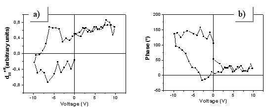
ensure that the fabricated nanostructures were ferroelectric, measurements were
carried out on them by Piezoresponse Force Microscopy (PFM). For this, samples
were deposited onto conductive Nb-doped (100)SrTiO3 substrates. Local
piezoelectric and phase hysteresis loops were measured in the regions of the
coating where the ~40 nm diameter particles showed an order (Fig.2).
Figure 2. Piezoresponse Force Microscopy. Piezoresponse of the
perovskite nanostructures prepared by the microemulsion aided sol-gel method
onto a conductive Nb doped SrTiO3 substrate. a) and b) Local
d33eff and phase
hysteresis loops, respectively, measured on the regions of the coating where
the ~40 nm diameter PbTiO3 particles show one dimensional
periodicity.
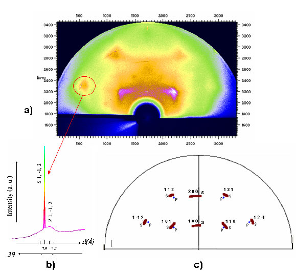
Figure 3. Synchrotron radiation grazing incidence scattering.
a) Experimental 2-D
diffraction pattern. Debye-rings' sectors and diffuse scattering maxima are
observed. b) Intensity profiles of a representative sharp-broad peaks pair. c)
Modeled 2-D diffraction pattern. Debye ring sections of the SrTiO3
substrate (colored wine) are denoted "S". The angular width of the ring
sections is approximately 10ş. The centers of broad PbTiO3
maxima (colored blue) are denoted "P". Lattice parameters:
SrTiO3 (space group P 4/m -3 2/m) a = 3.900 Ĺ;
PbTiO3 (space group P 4 m m) a = 3.8966 Ĺ, c =
4.1494 Ĺ.
The results shown here make these oxide nanostructures attractive for
applications in nanoelectronic devices, pointing to the proposed fabrication
strategy as a promising approach for the self-assembly of ferroelectric oxide
nanostructures, which, in principle, is applicable not only to ferroelectric
perovskites, but also to other functional multimetallic oxides.
Primary Citation
As the dimension of the microelectronic devices keep shrinking there is a press
ing need to increase the dielectric constant of the gate oxide. Fabrication of
the gate oxide out of ferroelectric nanostructure provides a possible solution.
However, new approaches to the fabrication of ferroelectric nanostructures
onto substrates are needed before nanoscale ferroelectrics can be
successfully integrated into functional microelectronic devices. An important
challenge is that the Sol fabrication of these materials in organized
arrangement of the nanostructures is reliable and very cost-effective.

In order to determine if the structural phase of the deposited nanostructures
was perovskite or not and to understand the crystallographic relationship to
the substrate, grazing incidence x-ray synchrotron radiation scattering
measurements were performed using an area detector at SSRL Beam Line 11-3. An
area detector has scarcely been used in the analysis of ferroelectric isolated
nanostructures or perovskite thin and ultrathin films. The two-dimensional
diffraction pattern obtained is shown in Figure 3a. It consists of sharp short
arcs and some diffuse spots. Figure 3b shows a 1D (line scan) cut through a
representative sharp-broad peak pair. The positions of the Sharp Debye arcs
agree well with the diffraction maxima of SrTiO3. The strong texture
of the measured the Debye arcs indicates that the SrTiO3 crystals
were orientated with (001) poles approximately normal to the sample surface.
The diffuse spots of Figure 3a always appear on the low angle side of the sharp
SrTiO3 arcs. This indicates a crystal phase with larger lattice
parameters than SrTiO3, but an identical crystal structure. These
maxima fit to PbTiO3 perovskite reflections well. The orientation
similarity of the substrate and the PbTiO3 phase indicates that the
PbTiO3 nanostructures have grown epitaxially on to the
SrTiO3 substrate. Further, from the semi-quantitative analysis of
the broadening of the peaks assigned to PbTiO3, it is deduced that
these structures have nanometric sizes, as previously observed from the
topographic image of Figure 1, and that they are strained. Modeling of all the
Debye arcs and broad spots maxima is depicted in Figure 3c. An angular width of
~10ş for the Debye arcs is assumed in the simulations.
M. L. Calzada, M. Torres, L. E. Fuentes-Cobas, A. Mehta, J. Ricote and L.
Pardo. (2007) Ferroelectric self-assembled PbTiO3 perovskite nanostructures
onto (100)SrTiO3 substrates from a novel microemulsion aided sol-gel
preparation. Nanotechnology. 18: 375603.
SSRL is supported by the Department of Energy, Office of Basic Energy Sciences. The SSRL Structural Molecular Biology Program is supported by the Department of Energy, Office of Biological and Environmental Research, and by the National Institutes of Health, National Center for Research Resources, Biomedical Technology Program, and the National Institute of General Medical Sciences.