
Charge density waves (CDW) are a type of coupled electronic-lattice instability
found in quasi-low dimensional materials. The driving force behind the
instability is the reduction in energy of electrons in the material as a
consequence of establishing a spontaneous periodic modulation of the
crystalline lattice with an appropriate wave vector. The symmetry of the CDW
state is very sensitive to the electronic structure of the host material.
Charge density wave has been observed in quasi-one dimensional compounds, high
temperature superconductors, manganites and many others.1-4 Conventionally, Fermi surface nesting is
the dominant and textbook mechanism for CDW. However, it fails to explain the
CDW in the 2H-structured transition metal dichalcogenides (2H-TMD's), which is
actually the first two-dimensional CDW materials discovered in 1975.5 Even after three decades of intensive research on this
subject, the CDW mechanism of 2H-TMD's remain mysterious and controversial.
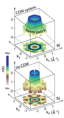
Figure 1. The photoemission intensity map taken at 15K for (a)
Na0.05TaS2 with CDW order below 65K, and (b)
Na0.1TaS2 without CDW order.
Utilizing the high-resolution ARPES apparatus at beamline 5-4 of SSRL,
scientists from the Department of Physics at Fudan University and SSRL have
recently successfully resolved this long-standing mystery. They investigated
the evolution of electronic structures of the 2H-NaxTaS2 compounds, where the
strength of CDW can be tuned upon adjusting the doping concentration of the
alkali metal elements.
They found that the strong electron-phonon coupling in this system makes the
electrons widely spread in the momentum space. At the Fermi energy, the states
locate not only at the conventional Fermi surfaces, but also over other large
regions in the Brillouin zone for the CDW samples, forming the so-called "Fermi
patches" (Figure 1); and the system with CDW order has more states over the
Fermi patches than the system without CDW order. Further experiments revealed
that a CDW gap opens over the Fermi patches, but not at the Fermi surfaces
around t as shown in Figure 2(a). This undoubtedly
indicates that the electronic states over the Fermi patches are responsible for
the CDW.
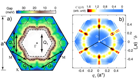
Figure 2. (a) The distribution of the CDW gap in the first Brillouin
zone of Na0.05TaS2. The dashed lines are the conventional Fermi surfaces. (b)
The two-dimensional joint density-of-states of the ARPES intensity in the
normal state of CDW65K. Q1, Q2, and
Q3 are the ordering wave-vectors.
Because many complex materials bare similar electronic properties, such as
Fermi patches and broad lineshapes, this Fermi-patch driven CDW mechanism may
be a general theme for charge ordering in the strong electron-phonon coupling
regime.
Primary Citation
References
To understand the unusual CDW transition, it is crucial to obtain a
comprehensive picture of the subtle low energy electronic structure changes
upon the CDW transition. Combining the state-of-the-art electron analyzer and
the intense photon beam from a synchrotron accelerator or a high flux helium
discharge lamp, modern angle-resolved photoemission spectroscopy (ARPES) can
now reach sufficiently high energy and momentum resolutions to address this
issue.
To explain the 3x3 CDW ordering in this material, the joint density-of-states
over the entire Brillouin zone was estimated [Figure 2(b)], which reflects the
phase space for charge instabilities.6 The peaks at
the right ordering wave-vectors prove that such charge ordering is indeed
favored by the collective behavior of all the states at the Fermi patches. In
this way, they resolved previous controversies and unveiled a new CDW mechanism
in this material, namely, the Fermi-patch mechanism.
D. W. Shen, B. P. Xie, J. F. Zhao, L. X. Yang, L. Fang, J. Shi, R. H. He, D. H.
Lu, H. H. Wen, D. L. Feng*, "Novel Mechanism of a Charge Density Wave in a
Transition Metal Dichalcogenide" Physical Review Letters 99, 216404 (2007).
SSRL is supported by the Department of Energy, Office of Basic Energy Sciences. The SSRL Structural Molecular Biology Program is supported by the Department of Energy, Office of Biological and Environmental Research, and by the National Institutes of Health, National Center for Research Resources, Biomedical Technology Program, and the National Institute of General Medical Sciences.