 Conjugated polymers are being developed as the active semiconductor in devices
such as light-emitting diodes, photovoltaic cells, and thin-film transistors
(TFTs) for large-area and low-cost electronics. Vacuum deposited amorphous
silicon is currently used in the TFTs that drive the active matrix liquid
crystal displays (AM-LCDs) on laptops, computer monitors and televisions. TFTs
are also used in disposable electronics such as radiofrequency identification
chips. Solution processible conjugated polymers, such as the polythiophenes,
can be deposited by low cost methods like inkjet and screen printing. The
charge carrier mobility (0.1 cm2/Vs) of the standard polythiophene,
poly(3-hexylthiophene) (P3HT), is just below that of amorphous silicon (0.6
cm2/Vs). To open up more applications and to better compete with
amorphous silicon, the mobility of polymer semiconductors needs to be improved.
The key to improving the mobility is to develop an understanding of the
relationship between polymer morphology and charge transport.
Conjugated polymers are being developed as the active semiconductor in devices
such as light-emitting diodes, photovoltaic cells, and thin-film transistors
(TFTs) for large-area and low-cost electronics. Vacuum deposited amorphous
silicon is currently used in the TFTs that drive the active matrix liquid
crystal displays (AM-LCDs) on laptops, computer monitors and televisions. TFTs
are also used in disposable electronics such as radiofrequency identification
chips. Solution processible conjugated polymers, such as the polythiophenes,
can be deposited by low cost methods like inkjet and screen printing. The
charge carrier mobility (0.1 cm2/Vs) of the standard polythiophene,
poly(3-hexylthiophene) (P3HT), is just below that of amorphous silicon (0.6
cm2/Vs). To open up more applications and to better compete with
amorphous silicon, the mobility of polymer semiconductors needs to be improved.
The key to improving the mobility is to develop an understanding of the
relationship between polymer morphology and charge transport.
 | |
|
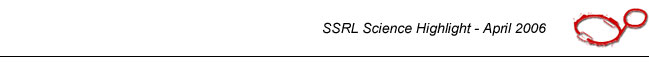
Figure 1 - a) plane-on and b) edge-on orientation of P3HT. |
  |
|
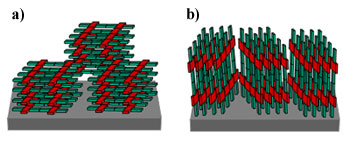
| Figure 2 - a) schematic of orientation of crystals within the film corresponding to the peak and background of the b) rocking curve of P3HT films. |
This same team of researchers in collaboration with scientists from Merck
Chemical and the Palo Alto Research Corporation (PARC) have revealed a new
polymer, poly(2,5-bis(3-alkylthiophen-2-yl)thieno[3,2-b]thiophenes)) (PBTTT),
with the highest reported charge carrier mobility (0.7 cm2/Vs) to date, making
it competitive with amorphous silicon. Measurements at SSRL and Stanford showed
the polymer to have the highest crystallinity ever observed for a
semiconducting polymer. The edge-on orientation of the polymer crystals was
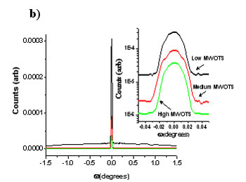
enhanced by annealing the films in the liquid crystalline regime. Atomic force
microscope images (figure 3) of these films showed crystal domain sizes on the
order of 200 nm, almost an order of magnitude larger than any previously
observed in semiconducting polymers. The specular diffraction intensity was
also over an order of magnitude higher than the best P3HT films. These results
showed that the films consisted entirely of the highly oriented crystals first
observed in P3HT. The researchers have shown the polymer to have a similar
morphology to what is seen in small molecules despite having polymer chains 40
times longer.
Figure 3 - Atomic force microscope image of grains of
pBTTT.
Primary Citations
"Highly Oriented Crystals at the Buried Interface in Polythiophene Thin Film
Transistors", R.J. Kline, M.D. McGehee, M.F. Toney, Nature Materials 5, 222-228
(2006).
"Liquid crystalline semiconducting polymers with high charge carrier mobility",
I. McCulloch, M. Heeney, C. Bailey, K. Genevicius, I. MacDonald, M. Shkunov, D.
Sparrowe, S. Tierney, R. Wagner, W. Zhang, M.L. Chabinyc, R.J. Kline, M.D.
McGehee, M.F. Toney, Nature Materials 5, 328-333 (2006).