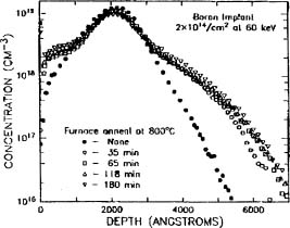

The nature of defects introduced by ion implantation and their subsequent interaction during high temperature processing with the implanted ion species is of considerable technological and recent scientific interest. If ion implantation is to continue being used for future device generations, it is imperative that we understand and attempt to control the phenomenon of Transient Enhanced Diffusion (TED). TED is observed upon annealing ion implanted silicon, we notice that the diffusion of the ion implanted species is enhanced by several orders of magnitude compared to the bulk diffusivity. In addition, the phenomenon is transient and of limited duration depending on time and temperature. The phenomenon is illustrated in Fig. 1 which shows the concentration profiles of Boron implanted silicon versus depth as a function of annealing time at 800°C. Note the saturation of the diffusion profile at long annealing times.
At SSRL we have initiated a program in collaboration with our industrial colleagues at Intel Corporation and scientific colleagues at the University of Munich, Stanford University, the University of Illinois and the Lawrence Livermore laboratories to try to understand in a systematic way the defects introduced by ion irradiation and their subsequent interaction with implanted ions.
In particular we concentrate on identifying and characterizing point defects and point defect clusters too small to be observed by transmission electron microscopy. A powerful method for detecting point defects or defect clusters is to analyze the diffuse scattering in the tails of Bragg peaks or the weak scattering between Bragg reflections. In metals the use of these methods allows unambiguous characterization of point defects and clusters such as dumbell pairs.
Since the implanted layers are usually about 2000 Å from the crystal surface we use grazing incidence geometry to restrict penetration and to suppress bulk scattering. The diffracting planes are normal to the (001) crystal surface. Both radial and angular scans were taken around the (400) and (220) Bragg peaks using a position sensitive detector to map out a region in reciprocal space around the Bragg tails.
In order to produce samples with a preponderance of one defect type we have adopted the following procedure for sample preparation. Floating zone dislocation-free silicon crystals were cleaned and implanted with a high Boron dose at 32 keV. The wafers were then Rapid Thermal Annealed (RTA) at 1070°C in order to anneal the implant damage and to locate the Boron predominantly in substitutional sites. The wafers were then implanted with a lower dose of Silicon at 80 keV and annealed at 750°C for various times. We expect that defects introduced by the silicon implant will be captured during annealing by the substitutional Boron already present and thus produce a defect population largely consisting of Boron, B-Si interstitial pairs or small clusters.
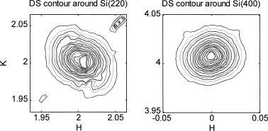
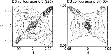
The contours of diffuse scattering around (400) and (220) Bragg peaks are shown in Fig. 2 for the crystal containing a high B concentration (6·1015 cm-2) annealed at 1070°C for 10 seconds after subsequent silicon implant (4·1014 cm-2) and annealing at 750°C for 10 sec. Besides the expected diffuse scattering around the (220) reflection, we notice a rather unusual feature. There are lobes of intensity displaced from the Bragg peak in the [220] direction. For the (400) reflection the peaks are not as clear, however, we can clearly see four lobes of intensity extending in the [-220] and the [220] directions. The intensity lobes are more clearly seen for crystals with an initial concentration of B (6·1014 cm-2) that is an order of magnitude less than the previous case shown in Fig. 2. After annealing at 1070°C for 10 sec. and subsequent Si implantation (2·1014 cm-2) anneal at 750°C 10 sec. the intensity contours for the (400) and (220) reflections are shown in Fig. 3. For the (220) reflection the lobes in the [220] direction are clearly visible. Around the (400) reflection four lobes of intensity are observed in the two {220} directions.
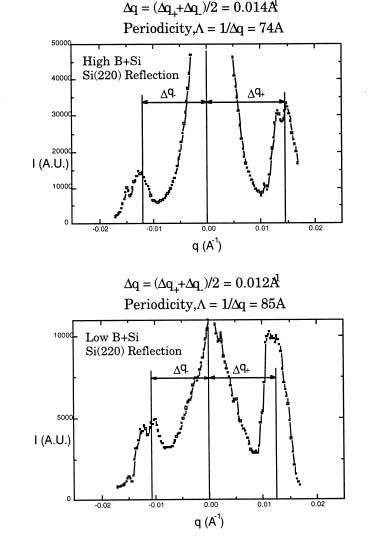
In Fig. 4 we plot the intensity profile for the high B sample in the [220] direction. Besides the tail of the (220) Bragg peak satellite peaks on either side of the main peak are clearly visible. From the spacing q of the satellite peaks we obtain a period distance of 74 Å for the high B sample shown in Fig. 4 (a). A similar profile for the low B sample shows satellite peaks somewhat lower in intensity and a periodicity of 85 Å. Fig. 4(b).
The results are internally consistent since the (400) reflection shows as would be expected pairs of satellite peaks in the [-220] and [220] directions. This is especially clear for the low B case and less so for the high B (220) results.
While the results clearly indicate a periodicity in the <220> directions, it is difficult at this stage to propose a model for the origin of these satellites. At present we can only speculate that the data are consistent with a lateral modulation normal to the surface on the scale of 75-85 Å. Since the implanted layer is only 2000 Å from the surface, a surface-mediated strain induced periodicity may be the cause for the observed satellites. We intend to look at reflections other than those investigated in this report to shed further light on this rather unexpected result.
The original aim of this work was to characterize the defects introduced by ion implantation by analyzing the diffuse intensity in the Bragg tails. To aid in the defect characterization we have used molecular dynamics simulation methods to predict the defect types and impurity profiles. The predicted profiles will be compared to experimentally obtained SIMS (Secondary Ion Mass Spectroscopy) profiles and refined to fit the experimental data. Preliminary work indicates that the defects are mainly point defects as well as B3I and B4I2 clusters, where (I) refers to interstitial silicon. Atomic displacements around such clusters have been calculated using first principles methods by our collaborators at the Lawrence Livermore National Laboratories. All of this information will be used to calculate directly the diffuse scattering under Bragg reflections and compared to the results we have in contour form in Figs. 2 and 3. Experimental verification of the simulation results is important since it will provide a sounder basis for the simulations and provide additional confidence for including such data in process codes that are widely utilized in the semiconductor industry.
Our colleagues in this rather extensive project are listed below since the format of this Newsletter does not allow an extensive author list. Much time and diligent effort has been expended by U. Beck and C. H. Chang in the experiments and data analysis. At Munich the support and participation of J. Peisl is gratefully acknowledged. We are grateful for a travel grant from NATO that made this cooperative effort possible.
Our close collaborators in the myriad problems raised in these studies are our Stanford colleagues P. B. Griffin and J. Plummer, at Lawrence Livermore T. Diaz de la Rubia and M. Caturla, at Illinois B. Averback and K. Nordlund and at Intel M. Giles and B. Doyle. The diffuse scattering experiments were carried out at ESRF, Grenoble and SSRL. We gratefully acknowledge the expert assistance of J. Arthur, S. Brennan and G. Grubel. Finally one of us (JRP) would like to thank J. Carruthers of Intel for suggesting the TED problem and his encouragement and support for this work.
|
|
Fig. 1. Boron profiles for several anneal times at 800°C. From A.E. Michel, W. Rausch, P.A. Ronsheim and R.H. Kastl, Appl. Phys. Lett., 50 , 416 (1987) |
|
Fig. 2: Contours of diffuse scattering intensity from silicon containing a high B concentration 6·1015 cm-2 annealed at 1070°C 10 sec. after subsequent silicon implant 4·1014 cm-2 and annealed at 750°C 10 sec. |
|
Fig. 3: Contours of diffuse scattering intensity from silicon containing a low B concentration 6·1014 cm-2 annealed 1070°C 10 sec. after subsequent silicon implant 2·1014 cm-2 and annealed at 750°C for 10 sec. |
|
Fig. 4 Intensity profile along (220) direction. (a) high Boron concentration; (b) low Boron concentration. |
 |