Organic semiconductors are attracting considerable research interest due to already commercialized and potential applications in low-cost electronics such as organic light emitting diode (OLED) displays, thin film transistors and related applications (e.g. TFT sensors), RF identification tags (RFID), smart cards electronic paper etc.). In the field of organic semiconductor research, the material pentacene has developed into a benchmark material because high-performance thin film transistor (TFT) devices are easily and robustly obtained from vacuum-deposited thin films of pentacene on a variety of substrates. Pentacene thin films on silicon oxide are a particularly interesting case because, despite their polycrystalline film morphology (i.e. structural imperfections and small grains), the pentacene TFTs outperform single crystal-based pentacene transistors. The key to understanding the electrical performance of pentacene TFTs lies with the first few layers of pentacene. When a TFT device is switched "on", the current flows predominantly in the first few molecular layers and the packing and exact arrangement of molecules in these layers determine the current obtained at an applied voltage. The knowledge of the precise packing in the first monolayer is, therefore, crucial to understanding the charge transport properties of pentacene TFTs.

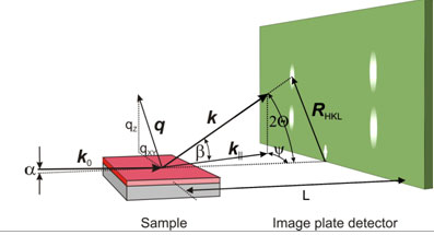
Pentacene sub-monolayer films were prepared by vacuum-deposition onto SiO2 substrates at 60°C, which are typical deposition parameters we use to produce high-performance TFTs. Grazing incidence X-ray diffraction (GIXD) with synchrotron light offers the unique opportunity to study the diffraction from weakly scattering, ultra-thin films such as a single molecular layer of pentacene. The scattering geometry of the GIXD experiment performed on SSRL's Beam Line 11-3 is depicted in Fig. 2. The incidence angle a of the incident beam k0 was set to 0.1°. The diffraction intensity was detected on a 2D image plate (MAR-345, distance L=402 mm).
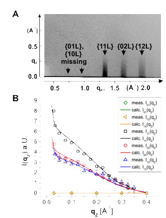
While the positions of the diffraction peaks recorded on the image plate provide information on the lattice geometry of the crystalline film, the brightness of the diffraction peaks contains information on the molecular orientation and packing within the lattice unit cell. In the case of a 2D crystal (e.g., a monolayer), discrete peaks are only observed "in-plane" (the qxy-direction in Figs. 2 and 3A). In the out of plane direction (the qZ-axis in

Fig. 3A), there is no limiting Bragg condition (because the film is a single layer thick) which leads to continuous scattering profiles (Bragg rods). These Bragg rod intensity profiles as obtained from GIXD on a single monolayer of pentacene were used to extract the alignment of the pentacene molecules.
The molecular packing that best explains the observed intensity profiles was extracted by numerical optimization of the differences between theoretical and observed diffraction intensities; the results not only reproduced the three visible intensity profiles with good accuracy, but also verified the experimentally observed absence of measurable diffraction intensity in the two first order in-plane diffraction profiles (labeled {01L} and {10L} in Fig 3A).
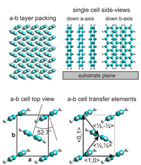
The packing motif of two pentacene molecules in the unit cell from the calculation procedure is shown in Fig. 4. Similar to previous reports investigating thicker pentacene films (20-50 nm), the pentacene molecules in the first monolayer form a so-called herringbone pattern (upper left panel in Fig. 4). However, in contrast to the thicker multilayer pentacene films, the molecules in the first monolayer stand exactly upright on the SiO2 surface. To compare the electronic properties of the monolayer arrangement with vertical pentacene molecules to the packing motif in bulk pentacene single crystals, DFT calculations were performed (for details refer to first reference below). The results of these calculations suggest that the upright configuration in conjunction with the slightly smaller unit cell in the pentacene monolayer (compared to bulk pentacene) lead to the high mobility values observed in pentacene films.

In summary, this work shows that it is possible to determine the exact structure in a single molecule-thick layer of organic semiconductor molecules using a combination of synchrotron-based X-ray diffraction and crystallographic refinement calculations. The monolayer structure we obtain explains the previously poorly understood excellent transport in polycrystalline pentacene films. The differences in the packing motifs of a pentacene monolayer and thicker pentacene films underline the importance of probing the relevant physical properties (e.g. structure) exactly at the location relevant to the properties that one desires to explain.
Further Reading
Thin film structure of tetraceno[2,3-b]thiophene characterized by grazing incidence X-ray scattering and near-edge X-ray absorption fine structure analysis, Q. Yuan, S.C.B. Mannsfeld, M.L. Tang, M.F. Toney, J. Lüning, Z. Bao, J. Am. Chem. Soc. 130, 3502 (2008).
Microstructure of Oligofluorene Asymmetric Derivatives in Organic Thin Film Transistors, Q. Yuan, S.C.B. Mannsfeld, M.L. Tang, M. Roberts, M.F. Toney, D.M. DeLongchamp, Z. Bao, Chem. Mater. 20, 2763 (2008).
Precise Structure of Pentacene Monolayers on Amorphous Silicon Oxide and Relation to Charge Transport, S.C.B Mannsfeld, A. Virkar, C. Reese, M.F. Toney, Z. Bao, Adv. Mat. 21, 2294 (2009).

