
Graphene, a two dimensional semi-metal made of sp2 hybridized carbon, is an outstanding material which exhibits high mechanical and chemical stability, as well as high charge carrier mobility. Graphene has recently received considerable attention because it can be directly integrated into opto-electronic devices, enabling the formation of efficient thin film and flexible devices.
There is a growing interest in “blending” graphene with semiconducting polymers in order to improve or enhance the properties of polymer based electronic devices. Due to their optical absorbance and their ability to transport charges, semiconducting polymers, such as the widely used poly-3- hexylthiophene (P3HT), have been successfully used in organic photovoltaic solar cells ((OPVs) and in field effect transistors (TFTs)). Thin films of these polymers are typically formed by spin-coating from solution onto a substrate. The properties of this thin polymer layer strongly depend on its crystallinity and internal nanostructure, which is partially determined by the interactions between the polymer chains and the substrate.
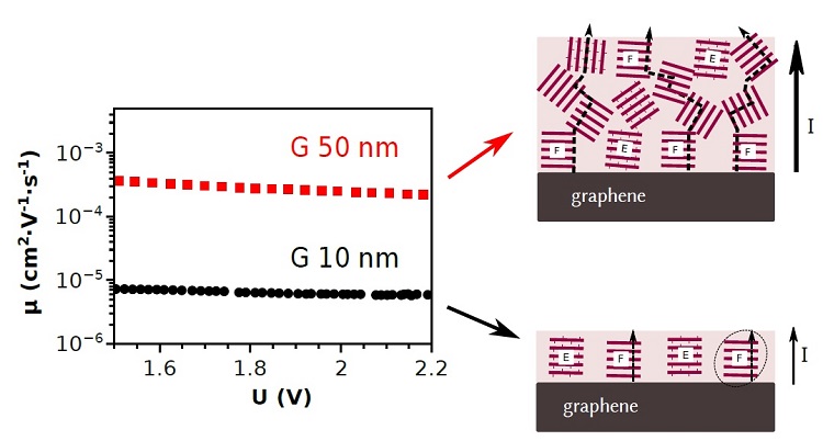
Due to strong interactions between the π orbitals in graphene and in the polymer, P3HT tends to form “face-on” lamellae, where the polymer chains lie flat on the substrate. This typically enables charge transport vertically through vertical π–π stacking. It is also widely believed that a thinner polymer film should enable faster and more efficient charge transport than a thicker one.
In a new study performed by an international team led by Prof. David Barbero from Umeå University in Sweden, the crystallization of highly regioregular P3HT thin films on top of a single layer of graphene was studied by grazing incidence X-ray diffraction at SSRL and compared to films deposited on a silicon substrate. The electronic properties of these films were also measured in Prof. Barbero’s lab, and showed that P3HT films deposited on graphene resulted in much enhanced vertical charge transport compared to films on silicon due to the stronger π–π interaction with the graphene substrate and the formation of vertical π–π stacked face-on lamellae.
However, a surprising result of this study was that the charge carrier mobility of a thicker P3HT film (50 nm) was approx. 50 times higher than in the case of an ultrathin P3HT film (10 nm) deposited on graphene. A thorough study of the crystallinity of these layers revealed that the ultrathin P3HT film formed well oriented face-on and edge-on lamellae, whereas the thicker film formed a mosaic of lamellae oriented at different angles from the graphene substrate.
This mosaic of crystallites with π–π stacking oriented homogeneously at various angles inside the film is believed to favor the creation of a continuous pathway of interconnected crystallites, and resulted in a strong enhancement in vertical charge transport and charge carrier mobility in the thicker P3HT film.
These results provide a better understanding of polythiophene crystallization on graphene, and should help the design of more efficient graphene based organic devices by control of the crystallinity of the semiconducting film.
V. Skrypnychuk, N. Boulanger, V. Yu, M. Hilke, S. C. B. Mannsfeld, M. F. Toney and D. R. Barbero, "Enhanced Vertical Charge Transport in a Semiconducting P3HT Thin Film on Single Layer Graphene", Adv. Funct. Mater. (2014), DOI: 10.1002/adfm.201403418.
