Here we give a brief review how, starting around 2000, x-rays have helped to solve a longstanding scientific problem in magnetism. We present only the “big picture” which is readily understandable even for the non-expert. A more thorough discussion is given in the book “Magnetism - From Fundamentals to Nanoscale Dynamics” by J. Stöhr and H. C. Siegmann (see http://www.springer.com/west/home/physics/condensed?SGWID=4-10104-22-100725344-0 ).
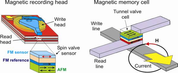
Some of the key magnetic devices found in advanced electronics like computers and MP3 players utilize an effect called “exchange bias” to pin (i.e. fix) the magnetization M of a ferromagnetic (FM) reference layer in a fixed direction in space. Relative to the fixed direction of M in the reference layer, o ne may then align the magnetization direction of a second ferromagnetic layer, called the sensor layer at an arbitrary angle. If the direction of M in the sensor layer is rotated by a magnetic field, the device acts as a sensor for the direction and strength of the magnetic field through the giant magnetoresistance effect, as utilized in magnetic recording heads and shown on the left of Fig. 1. If M in the sensor layer is used to define two distinct states, either parallel or antiparallel to the reference layer, we have a memory cell consisting of “1” and “0” bits, as shown on the right of Fig. 1. The key requir ement is to keep the reference layer unaffected by whatever one does with the sensor layer – and this is assured by exchange bias. In general, the effect is defined as the unidirectional pinning of a ferromagnetic layer by an adjacent antiferromagnet (AFM). For many years the ex change bias effect, discovered in 1956 by Meiklejohn and Bean, has been optimized through materials engineering and employed in devices without a good scientific understanding.
Fig. 1: On the left is shown a magnetic recording head, composed of a write head, containing a coil (yellow) and a yoke (blue) that guides the magnetic flux to a poin t where the emerging field magnetizes a magnetic disk that spins underneath. Embedded between insulators and shields is a magnetic read head, consisting of a spin valve sensor, that senses the small stray fields from the magnetic domains (bits) on the recording disk spinning underneath. The spin valve sensor consists of a FM reference layer whose magnetization direction is pinned by exchange bias to an AFM, and a sensor layer whose direction can be changed by a r elatively small field. On the right is shown the schematic structure of a magnetic memory cell, consisting of spin valve or tunnel valve. “1” and “0” bits consist of opposite magnetization directions of two ferromagnetic layers as in the spin valve on the left. The state of the cell is changed by the field of a current through the write line, and by sending a current through the read line, the “1” or “0” state of the cell is sensed by the giant or tunneling magnetoresistance effect.
The exchange bias effect is quite remarkable for several reasons. First, ordinary ferromagnetic meterials have not one but two equally favored magnetic directions, which are collinear and lie along the so-called "easy axis". Thus two equaly stable magnetization directions have the same energy, and the same magnitude of an external field is required to rotate the magnetization by 180° from one easy dirction to the other. As showwn on the left side of Fig. 2, the magnetization loop is therefore symmetric about zero field.
Second, the fact that exchange bias arises from the FM being in touch with an AFM is puzzling since we think of AFMs as magnetically neutral. Indeed when a ferromagnet is simply grown on top of an antiferromagnet the exchange coupling between the two systems only leads to an increased coercivity of the ferromagnet (Fig. 2 middle). This is usually attributed to the increased coercivity of “interfacial spins” which need to be dragged around by the external field. However, the ferromagnetic hysteresis loop is still symmetric, indicating two equivalent easy directions. If, on the other hand, the AFM-FM system is grown in a magnetic field or after growth is annealed in a magnetic field to temperatures above the AFM Néel temperature, the hysteresis loop becomes asymmetric and is shifted from zero (Fig. 2 right). This unidirectional shift is called exchange bias and reflects the fact that there is now a preferred easy magnetization direction for the FM. The magnetization M of the ferromagnet is pinned by the antiferromagnet into this direction.
In fact, for a properly designed exchange biased ferromagnet, the magnetization loop is shifted so much that after application of an external field in any direction, the remanent magnetization direction will always end up in the same direction. For example, as shown on the right side of ig. 1, M is always negative at remanence. Thus in a device consisting of a reference and a sensor layer, an external magnetic fields can only rotate or switch the sensor layer, but not the reference layer.

Fig. 2: Easy axis magnetization loops of a ferromagnetic (FM) film (left), a FM film grown on an antiferromagnet (AFM) (middle), and a FM/AFM sandwich prepared in a setting field Hset (right). In the right structure the FM is said to be biased with a bias field HB. The bias field points to the right, while the preferred direction of M points to the left, since the structure switches easier into this direction. Note that the loop may also be asymmetric vertically because some pinned moments do not rotate into t he direction ofHB, i.e. they remain aligned along the preferred direction of M.
From a scientific point of view the exchange bias phenomenon has been so fascinating because it clearly cannot be a bulk effect but must be due to the magnetic structure near the AFM-FM inte rface. Conceptually, the exchange bias corresponds to an exchange field, of the size of the bias field HB, transferred from the surface of the AFM into the FM. If one assumed an ideal magnetic structure of the AFM where all moments at the AFM/FM interface pointed in one direction as shown on the bottom left in Fig. 1, one might expect that the transferred exchange field may be as large as 10 Tesla [T]. In practice, however, the observed bias fields are only of order of 0.1 T or less. After closer inspection, it is therefore not the presence of a bias field but the small size of it that is puzzling!
For many years, the research on exchange bias was thus fueled by the search for structures with much larger bias fields. Exchange fields come free of charge and are equivalent to regular magnetic fields in their action on the spin part of the magnetization. Historically, the main problem in establishing a realistic model of exchange bias was the lack of information on the spin structure near the all-important interface, and owing to the difficulty of experimentally determining the magnetic structure right near the interface, the exchange bias puzzle remain ed unsolved for nearly 50 years. While even today new aspects of this phenomenon are still discovered, we will discuss here how over the last few years x-ray dichroism spectroscopy and microscopy measurements have made key contributions to the solution of the long-standing puzzle by providing direct information on the magnetic structure on both sides of the interface, linking FM and AFM structure, and on the interface itself. We now have a realistic model of exchange bias which appears to describe rea listic structures that are used in today’s devices. Such devices operate at room temperature and do not exhibit special “magnetic frustration” effects that may be frozen in at low temperatures.
An important historical challenge that was overcome by x-ray techniques was the direct imaging of AFM domains in thin films. While the AFM domain structure in bulk single crystals was studied already in the late 1950's little was known about the domain structure in thin films. For example, in well annealed bulk NiO the typical domain size is in the 0.1 - 1 mm range whereas in epitaxial NiO films the domain size is less than 50 nm. This size is below the spatial resolution of neutron diffraction topography (about 70 mm), x-ray diffraction topography (1-2 mm) and the fundamental resolution limit (about 0.2 mm) set by diffraction for optical and non-linear optical techniques. The importance of the antiferromagnetic domain structure is that on a microscopic level the exchange coupling across the AFM/FM interface is expected to proceed domain by domain and the correlation of the AFM with the FM domain structure is therefore of crucial importance.
A second key challenge solved by x-rays was the determination of the interfacial spin structure and its relationship with that in the AFM and FM films. As illustrated in Fig. 3, the use of x-ray absorption spectroscopy and microscopy techniques based on electron yield detection allows one to obtain unique information on the interface between a thin ferromagnetic layer on top of an antiferromaget. By tuning the photon energy one can tune into specific layers because of th e elemental and chemical specificity of XAS. X-ray polarization control opens the door for magnetic studies by means of x-ray magnetic linear dichroism (XMLD) on antiferromagnets, and x-ray magnetic circular dichroism (XMCD) on ferro- and ferri-magnets. Electron yield detection provides limited sampling depth, and for thin film sandwiches the signal contains a sizeable interface contribution. The well-known capability of full field imaging by use of an electron microscope, called XPEEM, offers high spatial resolution and allows observation of the exchange coupling and biasing effects, domain by domain. XPEEM combines two well-established concepts, polarized x-ray absorption spectroscopy (XAS) and electron microscopy into a spectro-microscopy technique.

Fig. 3: Illustration of unique capabilities utilized in x-ray dichroism spectroscopy and microscopy. On the left we show the elemental specificity of x-ray absorption spectroscopy. In the middle is illustrated the ability to distinguish magnetic domains through the polarization dependent intensities of cha racteristic L-edge resonances. For ferromagnets like Co the intensity depends on the projection of the magnetic direction relative to the photon angular momentum of the circular polarized x-rays (XMCD). For antiferromagnets like NiO the intensity depends on the angle of the magnetis axis relative to the E vector of linear polarized x-rays (XMLD). On the right we show the layer-by-layer electron yield contribution which decays with a 1/e sampling depth of about 2 nm into the bulk. An interface near the surface (red) gives a finite contribution.
The puzzle about the origin of uncompensated spins was solved by the experimental demonstration that real interfaces differ significantly from ideal, abrupt, single-step AFM–FM junctions between bulk-like crystal and spin structures. In particular, x-ray measurements gave the following key insights:
Below we shall illustrate these points by selected results of x-ray measurements.
1. Alignment of Magnetic Domains [1-5]
We start with presenting in Fig. 4 a comparison of the ferromagnetic domain structures of a thin film of Co with the antiferromagnetic domain structure of a NiO(100) single crystal underneath on which it was deposited. It is clear that the FM Co domain structure is determined by that of the AFM NiO underneath, directly showing that the magnetically neutral AFM “talks to” the FM. We also see that the FM moments are aligned along the AFM axis, proving point one above.

Fig. 4: On the left is show n the structure of the studied sample, consisting of eight monolayers of Co on NiO(001). The middle column shows polarization dependent x-ray absorption spectra recorded with circular polarization at the Co L3-edge and with linear polarization at the Ni L2-edge. The color-coded spectra were recorded for the corresponding color-coded areas in the XMCD and XMLD images shown on the right. The images on the right were recorded by PEEM. Arrows a nd wavy lines in the insets indicate the directions of the crystallographic axes and photon wave vectors, respectively. The directions of the magnetic moments in the domains are indicated by arrows. The AFM contrast in NiO was obtained by division of two XMLD images obtained with horizontally polarized light and photon energies correspo nding to the two L2-edge peaks. The FM image for Co was obtained by division of XMCD images recorded at the L3 and L2-edge energies. The magnetization direction of the Co film is found to be either parallel or antiparallel to the domains in the AFM, depending on which of the two AFM sublattices are present at the interface to Co.
2. Uncompensated Interfacial Spins [6, 7]
Close inspection of the x-ray absorption spectra for a Co/NiO sandwich, reveals that the Co L-edge spectrum shows a slight oxidation of Co metal and the Ni spectrum shows a slight reduction of NiO, as illustrated on the right side Fig. 5. This indicates interfacial interdiffusion of oxygen, resulting in an interfacial region that is about one monolayer thick. Pure NiO does not exhibit any XMCD signal because all Ni spins are completely compensated. However, the Co/NiO s andwich exhibits a ferromagnetic Ni signal, arising from Ni atoms with incomplete oxygen coordination. One can even image the uncompensated Ni spins by means of XMCD microscopy, as shown on the left side of Fig. 4. In the images on the far left the antiferromagnetic axis in the NiO substrate was chosen to be at 45o with respect to the incoming X-ray direction and the E-vector so that no AFM contrast is seen and the ferromagnetic X MCD contrast is more clearly revealed. In the middle panel the sample was rotated by 45o so that the AFM domains in NiO are now visible. The results of Fig. 5 therefore demonstrate the second point above.

Fig. 5: On the left are shown PEEM images, recorded for two orientations of the single crystal NiO(100) substrate relative to the incident x-ray beam. The photon energy was tuned to the Co absorption edge for the top images (blue frame) and to the Ni absorption edge for the lower images (red and green frames), and selecting the polarization for ferromagnetic (XMCD) and antiferromagnetic (XMLD) contrast, as indicated. From top to bottom, the domain structure reflects that seen for the fe rromagnetic Co layer, the ferromagnetic NiCoOx interface layer and that of the antiferromagnetic NiO(001) crystal substrate. On the right we show in red the Co and Ni L3 near-edge x-ray absorption fine structure recorded for the same sample. Comparison with reference spectra of pure CoO and Co metal and pure NiO and Ni metal, indicates that interfacial mixing has created a NiCoOx interfacial layer.
3. Pinned Interfacial Spins [8]
By use of careful field-dependent measurements on an exchange bias system, x-rays showed that not all uncompensated interfacial spins contribute in the same way. Only the pinned fraction creates bias while the other uncompensated interfacial spins contribute to the coercivity. The pinned moments can be separated by recording an element specific magnetization group of the uncompensated interfacial spins. This is demonstrated in Fig. 6 for the exchange bias system Co/IrMn. By use of the element-specific XMCD signal as a measure of the Co and Mn magnetic moments, one can obtain element-specific magnetization loops. In particular, the Mn loop is found to exhibit a horizontal as well as a vertical shift. From the vertical shift one finds that most Mn moments follow the field (and the moments in the Co FM) but a small fraction remains pinned in the direction opposite to HB, in accordance with Fig. 2. Quantitative analysis shows that the total number of uncompensated Mn moments corresponds to about 60% of a monolayer at the FM–AFM interface, and that about 7% of them are pinned. Thus the tiny amount of only 4% of a monolayer of pinned Mn moments are responsible for the entire exchange bias effect! This illustrates why it took so long to unravel the puzzle and supports the third point above.

Fig. 6: On the top we show two experimental geometries for XMCD hysteresis loop me asurements which differ in the alignment of the bias field direction HB relative to the angular momentum of the circularly polarized x-rays. On the bottom are shown measured XMCD hysteresis loops for Co and Mn atoms in exchange-biased Co/IrMn (2nm Co on 50nm of Ir20Mn80) samples for the two geometries. The dashed curve is for an unbia sed sample. The vertical offset in the Mn loops is due to pinned interfacial moments that do not follow the applied magnetic field. As shown in Fig. 2, these moments are aligned in the direction opposite to HB and thus contribute asymmetrically to the measured XMCD signal.
4. Domain Size [3, 10]
One of the important theoretical predictions about the size of exchange bias was developed in 1987 by Malozemoff, who used a random field model and a statistical treatment of the AFM domain size to show that the bias field HB should increase with decreasing AFM domain size d as 1/d. Such a beha vior was indeed found in 1997 by Takano et al. in a study of polycrystalline CoO/Ni81Fe19 films, prepared with different CoO grain sizes. However, to touch base with Malezemoff’s theory they had to assume that the grain size in antiferromagnetic CoO is equal to the AFM domain size. The ability to directly image small AFM domains by XMLD microscopy has allowed verification of this hypothesis. Results for the domain-size-dependent bias of the Co on LaFeO3 exchange bias system are shown Fig. 7. These measurements indeed confirm the conjecture of a 1/d domain-size-dependent exchange bias, supporting the fourth point above.

Fig. 7: By use of Co L-edge XMCD domain images of Co(1.2nm)/LaFeO3(40nm)/SrTiO3(001), recorded with PEEM as a function of an applied external magnetic field, one can obtain local remanent magnetization loops of the various Co domains. Two such loops are shown in pink and green on the top left. They show opposite bias directions despite the fact that no macroscopic bias was set. A magnetization loop that averages over domains shows no bias, as expected. On the top right we show a map of the local bias field extracted from the local magnetization loops for the various domains. As indicated by the color map, the local bias fields have a maximum values of ±30 Oe. Dependence of the local bias field on the domain area and domain diameter d reveal an inverse linear relationship 1/d, as shown at the bottom.
5. AFM Domain Wall [9]
Another important ingredient of the exchange bias puzzle is the role of the “bulk” AFM. Th e pinned interfacial spins are anchored deep in the AFM and for optimum bias the AFM must be magnetically hard, so that the AFM lattice can be considered rigid. If the AFM is soft, the AFM axis near the interface may partly rotate with the “pinned” interfacial moments when the FM is rotated by an external magnetic field. This would reduce the effective bias field. That the AFM can indeed rotate is revealed by Fig. 8, which shows a measurement of the orientation of the AFM axis in NiO for the Co/NiO(1 00) system in the presence of a magnetic field H of variable strength. The field was applied in the plane of the interface, parallel and perpendicular to the fixed direction of the x-ray polarization vector E,and the peak ratio of the Ni L2 –edge was used to monitor the relative orientation of the AFM axis relative to E. Since the measurements were performed by electron yield detection, the Ni signal predominantly originates from the NiO layers near the interface. Analysis of the data allows one to determine the degree of rotation of the AFM axis near the interface, revealing the winding up of a domain wall (see Fig. 9 below). One may interpret the plot of the AFM rotation as a function of f ield as the antiferromagnetic pendant to a ferromagnetic hysteresis loop. Such a loop cannot be observed for a bare AFM since the AFM axis does not rotate continuously in an applied magnetic field but will abruptly “flop” by 90o in a very large magnetic field. The existence of a planar antiferromagnetic domain wall, proven by the measurement, is a key assumption of most exchange bias models, as discussed below. This observation supports point 5 above.

Fig. 8 On the left are shown polarization-dependent Ni L2-edge x-ray absorption spectra for a sample of 2.5 nm Co/NiO(001) and the two experimental geometries illustrated in the middle of the figure. The x-rays were incident along the surface normal a nd an in-plane field of 0.7 T was applied. The difference of the two spectra is shown on the lower left. The intensity ratio of peak A to peak B is sensitive to the orientation of the AFM axis and can be used to determine how its orientation changes under the influence of an applied field. In each case, only one of the two orthogonal AFM domains in NiO rotates as shown in the middle. On the right we show how the peak intens ity ratio A/B changes with applied field for H perpendicular (empty squares) and parallel (filled squares) to the x-ray polarization vector E. The deduced rotation angle of the AFM wall (right abscissa) is plotted as circles. A fit based on a planar domain wall model (thick line) reprodu ces the data.
The various x-ray observations can be cast into a model for the exchange bias effect. The simplest model that accounts for the experimental observations is the Mauri-Siegmann model, depicted in Fig. 9.

Fig. 9: Mauri-Siegmann model of exchange bia s which contains all important features identified by x-ray experiments. A FM film of thickness t is separated by an interface of thickness ξ from a thick AFM below. The uniaxial anisotropy of the AFM is along x and there is parallel coupling between the uncompensated interfacial moments and the FM moments. The external magnetic field His applied at an angle β with respect to x and the FM moments are aligned parallel to H. Near the interface the AFM axis may rotate and form a domain wall. The rotation of the AFM axis in the domain wall is given by α ≤ β, and depends on the magnetocrystalline anisotropy of the AFM.
In the model, the anisotropy direction of the bulk AFM sets a preferred alignment direction for the AFM spins in the bulk, labeled x. In accordance with experimental observations there is an interface layer of thickness ξ (about one monolayer) which contains uncompensated spins that are aligned parallel to the AFM spin axis at the interface and are also parallel to those in the FM layer on top. A fraction of these interfacial spins are pinned, that means they are anchored deep in the bulk of the AFM. If we now apply a magnetic field H at an angle b with respect to the direction x, the FM moments will align along H, as shown. If the AFM is very hard there will be no twist of the AFM axis and the uncompensated interfacial spins will remain aligned unidirectionally along x. This is the case of maximum bias. If the AFM is soft, an exchange spring will form in the AFM. At the interface the uncompensated interfacial spins will be aligned along the AFM axis, at an angle a with respect to x, but they will twist until they become parallel to x in the bulk. If the interfacial spins can rotate in the field, the effective bias field will be reduced.
In this model the exchange bias field is determined by three key parameters. The first is the pinned interfacial moment density SA /(ξa), where SA the magnitude of the pinned interfacial spins, and ξ and a are the interface thickness and in-plane atomic separation, respectively. Secondly, two energies play a key role. One is the interfacial coupling energy density, given by EIF = J SASF /(ξa), where SF is the magnitude of the FM spin s, and J is the interfacial exchange coupling constant. The other is the AFM domain wall energy density EW. If the domain wall energy is large, EW > EIF, the AFM is rigid, preventing the winding up of a domain wall in the AF M. This is the case of maximum bias, given by HB = J SASF /(ξaMt), where t and M are the thickness and magnetization of the FM. If the domain wall energy becomes weaker than the interface exchange energy, EW < EIF , the bias field is determined by the formation of a domain wall and is given by HB = EW /(M t). This latter situation is the origin of the relatively weak bias field in NiO, which has a rather small magnetocrystalline anisotropy.
Since x-rays show that the pinned moment density is only a fraction of a monolayer, the exchange bias field HB is produced by few spins only, and is strongly reduced relative to that for an ideal, uncompensated interface. This explains why the bias is about a factor of 100 smaller than in early models, which assumed that a full monolayer of pinned interfacial spins is active in exchange bias. This model is very much in agreement with observations. The new observations employing XMCD have thus led to a valuable and useful understanding of exchange bias on the level of the chemical and physic al properties of the atoms at the interface. The best bias materials like IrMn are hard AFMs, while softer materials like NiO exhibit a reduced exchange bias effect.