
Katharina Lüning, Sean Brennan and Piero Pianetta SSRL/SLAC
 |
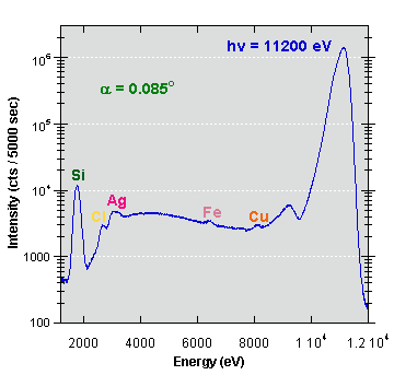 | |
| Figure 1: TXRF spectrum of a clean Si wafer surface showing 6.4x10⁸ atoms/cm2 Fe and 2.6x10⁸ atoms/cm2 Cu. The Cl is a residue from the HCl solution used to clean the wafer surface and the Ag is a artifact from the particular collimator used in these studies. Other features seen in the spectrum are the Si substrate peak, the scatter peak at 11.2 keV and the escape peak at 9.4 keV. | |
Apart from the detection of transition metals, SR-TXRF can also be extended to detecting elements with Z < 14, of particular importance is Al. This is not only challenging because of the smaller fluorescence yield as compared to transition metals, but especially because of the much stronger Si substrate fluorescence signal, which cannot be attenuated by a cut-off filter and therefore easily dominates the spectrum and saturates the semiconductor detector. Only exploiting the tunability of SR and choosing an excitation energy below the Si K absorption threshold can overcome these limitations. However, as shown in Figure 2, a substantial increase in background due to inelastic x-ray Raman scattering is observed. This background limits the minimum detection limit for Al, which has been derived for a bending magnet beam line to be 7.6x10⁹ atoms/cm2 for a standard 1000 s counting time [3].
Furthermore, the chemical state of device impurities can be investigated at trace levels by combining TXRF with x-ray absorption near edge spectroscopy (XANES) to monitor fluorescence yield as a function of excitation energy. Especially in case of semiconductor surfaces, the effect of an impurity strongly depends on its oxidation state and it is demonstrated that this technique will eventually contribute to the development of more efficient wafer cleaning processes.
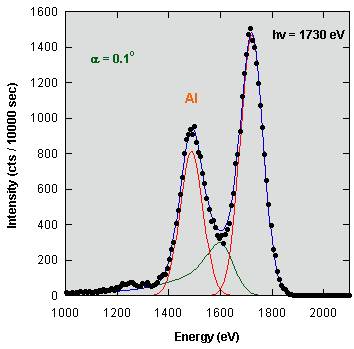 | Figure 2: Fluorescence spectrum (dots) from a Si wafer containing 3x10¹¹ atoms/cm2 Al. The modeled profile of the x-ray Raman scattering is shown (green), as well as the Gaussian fits for the aluminum signal (red) and the elastically scattered SR (red). The sum of the Gaussian fit and the Raman profile representing the simulated spectrum is shown in blue. |
This research was carried out at the Stanford Synchrotron Radiation Laboratory,
a national user facility operated by Stanford University on behalf of the U.S.
Department of Energy, Office of Basic Energy Sciences.
References
- K. Baur, S. Brennan, P. Pianetta, R. Opila, Anal. Chem. 74, 609-616 (2002).
- P. Pianetta, K. Baur, A. Singh, S. Brennan, J. Kerner, D. Werho, J. Wang, Thin Solid Films 373, 222-226 (2000).
- K. Baur, J. Kerner, S. Brennan, A. Singh, P. Pianetta, J. Appl. Phys. 88, 4642-4647 (2000).
SSRL Highlights Archive
